EUV light wavelength
Resolution
Projection optics
Wafers per hour
At dose: 50 mJ/cm²
Key features & benefits
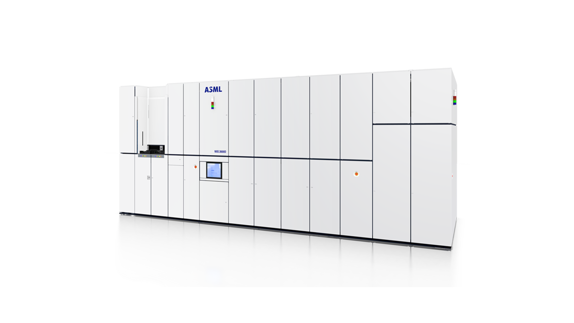
The TWINSCAN EXE:5000 is the first 0.55 NA, or ‘High NA’, EUV lithography system. Its 8 nm resolution will enable chipmakers to print with a single exposure features 1.7 times smaller – and therefore achieve transistor densities 2.9 times higher – than those possible using TWINSCAN NXE systems.
Because the EXE:5000 prints smaller features, chipmakers can reduce process complexity in high-volume manufacturing by using single instead of multiple patterning. This increases the wafer output in customer fabs by reducing production cycle time. The technology will enable multiple future chip architectures, starting at the 2 nm Logic node and followed by Memory nodes at a similar transistor density.
With 40% more imaging contrast than NXE systems, the EXE:5000 reduces the number of patterned defects that could impact chip performance. In addition it allows chipmakers to reduce the amount of light per exposure, or dose. That reduces the time required to print each layer and, by doing so, increases wafer output in customer fabs.
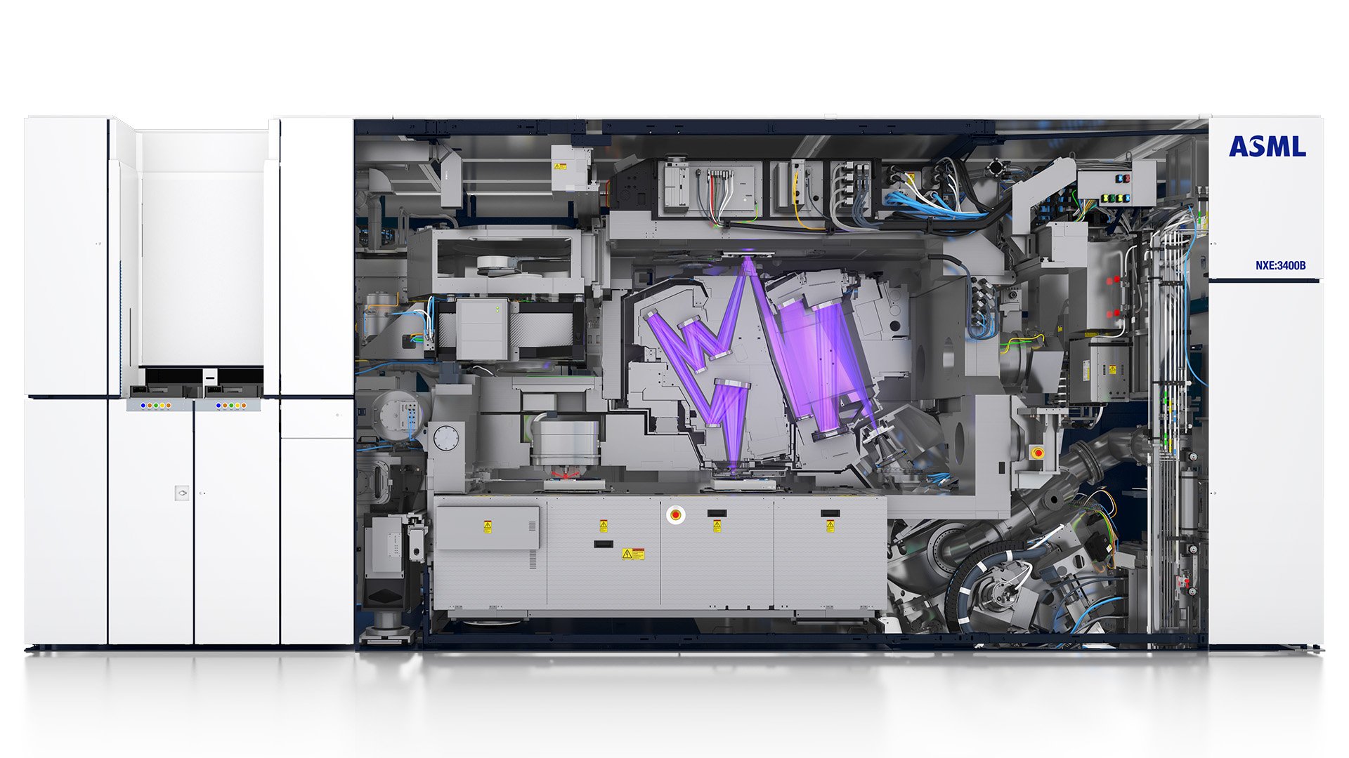
The system’s numerical aperture (NA) of 0.55 is enabled by new, larger projection optics. These so-called anamorphic optics provide the best imaging while allowing chipmakers to continue using traditionally sized reticles, thereby minimizing the technology’s impact on the semiconductor ecosystem.
The anamorphic mirrors require an exposure field half the size of that in NXE systems, which have an NA of 0.33. The EXE:5000 therefore has new, faster wafer and reticle stages to achieve the highest productivity and maintain the economic viability of producing future chip generations.