Pixel size
Field of view (pixels)
CD metrology precision
Defect detection capability
Key features & benefits
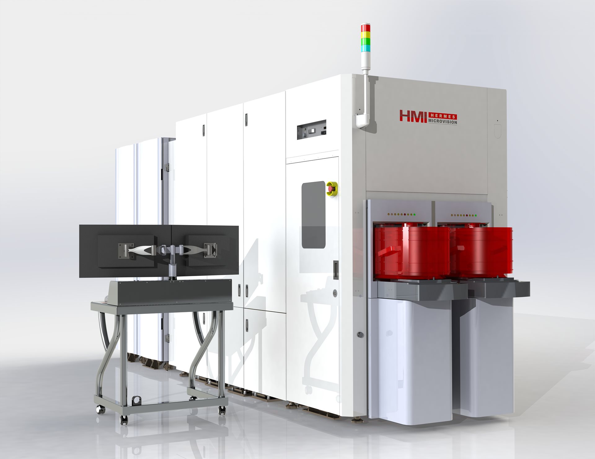
Our highest-resolution e-beam system to date, the eP5 offers critical dimension (CD) metrology and defect detection at high throughput.
The eP5 is as at home in the fab as it is in the R&D lab, allowing chipmakers to monitor process performance in production and verify optical proximity correction (OPC) models in development.
01. Versatility
The eP5 combines precise CD metrology with high-resolution defect detection in one system. For wafer inspection, it can operate in both physical defect and voltage contrast mode to detect patterning and electrical defects.
02. Sensitivity
With a 1 nm pixel size, the eP5 is our highest-resolution e-beam system. It is capable of detecting defects down to 5 nm and achieves < 0.1 nm CD precision with 0.05 nm measurement sensitivity. It offers industry-leading auto defect classification (ADC), while our die-to-database (D2DB) feature uses design information to further improve defect sensitivity and classification.
03. Throughput
A large (12,000 x 12,000 pixel) field of view enables high scanning throughput. Additionally, the eP5 can carry out CD metrology and wafer inspection at the same time to maximize productivity.
Pattern fidelity metrology option
The pattern fidelity metrology option available on the eP5 allows chipmakers to harness the superfine resolution of e-beam solutions at even greater throughputs to monitor high-volume production processes.
The option draws data from a wide variety of sources including our TWINSCAN lithography systems, our optical YieldStar and computational metrology systems, and the eP5 itself as well as our computational lithography solutions and non-ASML equipment.
It then analyzes this data to identify hotspots where defects are most probable, using this insight to guide and optimize scan strategies in the eP5. This allows chipmakers to maximize inspection throughput while still detecting yield-limiting defects.