Key features & benefits
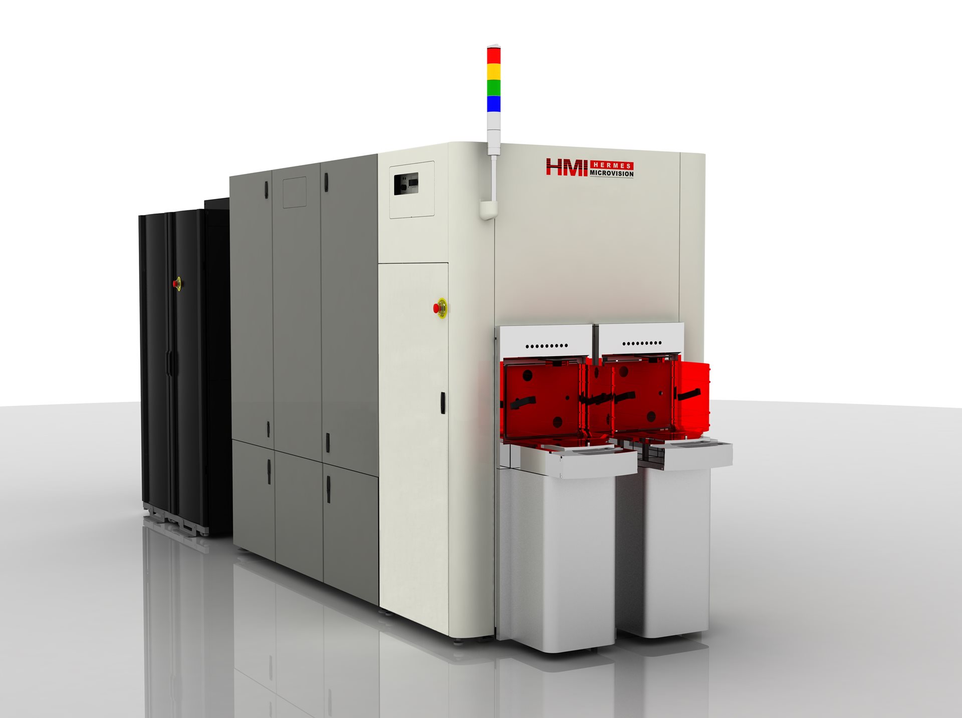
The eScan 600 is a highly flexible e-beam wafer inspection system that can operate in multiple modes, allowing chipmakers to capture the widest variety of defect types in a single system.
Together with a high throughput and superfine detection resolution, this versatility helps cut the cost of chip R&D and ramp-up.
01. Versatility
The eScan 600 can be used for physical defect inspection, voltage contrast defect inspection and material contrast defect inspection in backscattered electron (BSE) mode. This means that patterning defects, electrical defects (including open, short and leakage defects) and material contrast defects can be detected with just one system.
02. Sensitivity
The eScan 600 offers extremely high defect detection resolution to identify sub-design rule patterning defects. For instance, it can detect physical defects just a few nanometers in size, enabling efficient R&D for the most advanced microchips. In addition, GDS (graphic design system) assisted features such as GDS pattern-of-interest and GDS binning use design information to enhance defect sensitivity and classification. The eScan 600 can also be connected to SuperNova to support online die-to-database (D2DB) inspection, which uses additional design information to further improve sensitivity.
03. Throughput
The eScan 600 includes a number of features to increase the inspection throughput. Our patented technology enables a uniquely large field of view (120 µm x 120 µm) to increase throughput in leap-and-scan mode without harming sensitivity. The continuous scan mode provides high throughput inspection for voltage contrast and larger physical defects, while the SkyScan mode allows millions of patterns-of-interest in pre-identified locations to be scanned in just a few hours.