Key features & benefits
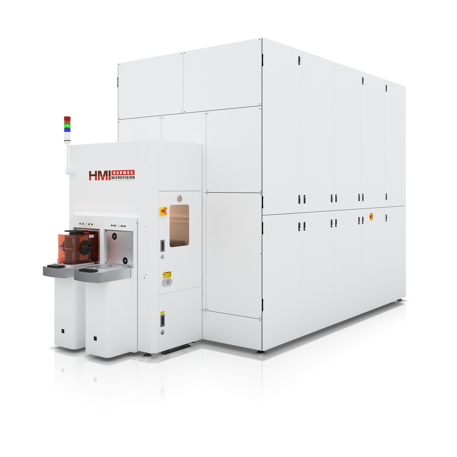
Following in the footsteps of the eScan 1000, the eScan 1100 offers new levels of efficiency in high throughput wafer inspection.
Targeting the 3 nm node and beyond, the eScan 1100 is the first generation of systems in our multibeam roadmap to bring high-throughput, high-resolution e-beam inspection into volume manufacturing environments.
01. Throughput
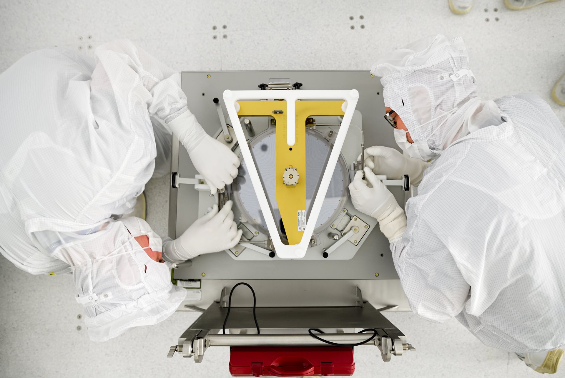
With 25 beams, the eScan 1100 will increase throughput by up to 15 times compared to single e-beam inspection tools, thanks to its multibeam technology, a high-speed wafer stage and advanced computational algorithms.
02. Key technologies
Compared to the eScan 1000, the eScan 1100 includes an improved electron optics system capable of creating and controlling 25 primary electron beams with higher resolution, collecting and processing the resulting secondary electrons, minimizing beam-to-beam crosstalk, and delivering consistent imaging quality across all beams.
It also features a high-speed stage to increase the system’s overall throughput and a high-speed computational architecture to process the streams of data from the multiple beamlets in real time. Advanced charging control (ACC) and high-voltage flooding technology provides comprehensive charging control capabilities to handle challenging voltage contrast inspection layers from Logic and Memory devices.
Additionally, its proprietary die-to-database defect detection capability enables chipmakers to further enhance defect sensitivity and to monitor EUV mask defects using wafer print check. It is capable of detecting defects overlooked by optical inspection systems in a fraction of the time that it takes single e-beam solutions, enabling a broader adoption of multibeam inspection in high-volume manufacturing.
03. Multimode operation
The eScan 1100 can be used for both voltage contrast defect inspection and physical defect inspection. This allows it to detect electrical defects (including open, short and leakage defects) and patterning defects down to 7 nm.