Key features & benefits
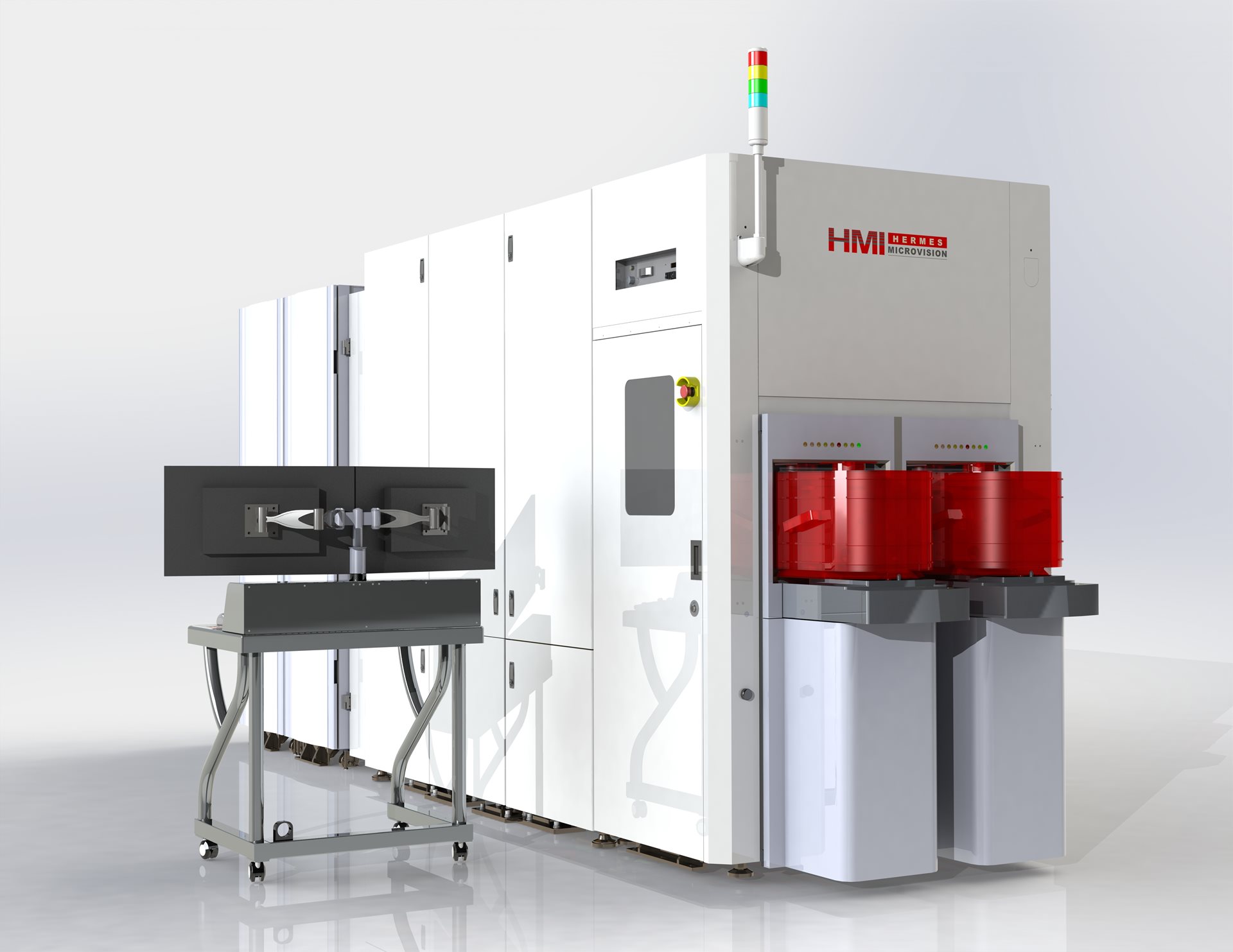
The HMI eScan 430 is a high-throughput e-beam wafer inspection system, capable of detecting patterning and electrical defects.
High sensitivity to multiple defect types combined with the fastest scanning available makes this system ideally suited to process monitoring in volume production as well process development in the R&D phase.
With its unique charging control design, the eScan 430 is the premier solution for monitoring 3D NAND production processes, and also supports the manufacturing of advanced DRAM and 3DXpoint memory chips.
01. Versatility
The eScan 430 can operate in both continuous-scan and hot-area mode, allowing it to detect voltage contrast defects at very high speed and physical defects with high sensitivity.
02. Sensitivity
The eScan 430 offers excellent defect detection resolution. It can detect physical defects below 10 nm and electrical failures such as open and leakage defects. In addition, GDS (graphic design system) assisted features such as GDS pattern-of-interest and GDS binning use design information to enhance defect sensitivity and classification. The eScan 600 can also be connected to SuperNova to support online die-to-database (D2DB) inspection, which uses additional design information to further improve sensitivity.
03. Throughput
The eScan 430 is uniquely able to scan up to a thousand square millimeters per hour for voltage contrast inspections. This allows chipmakers to collect more data about their production process and the performance of their wafers.