Key features & benefits
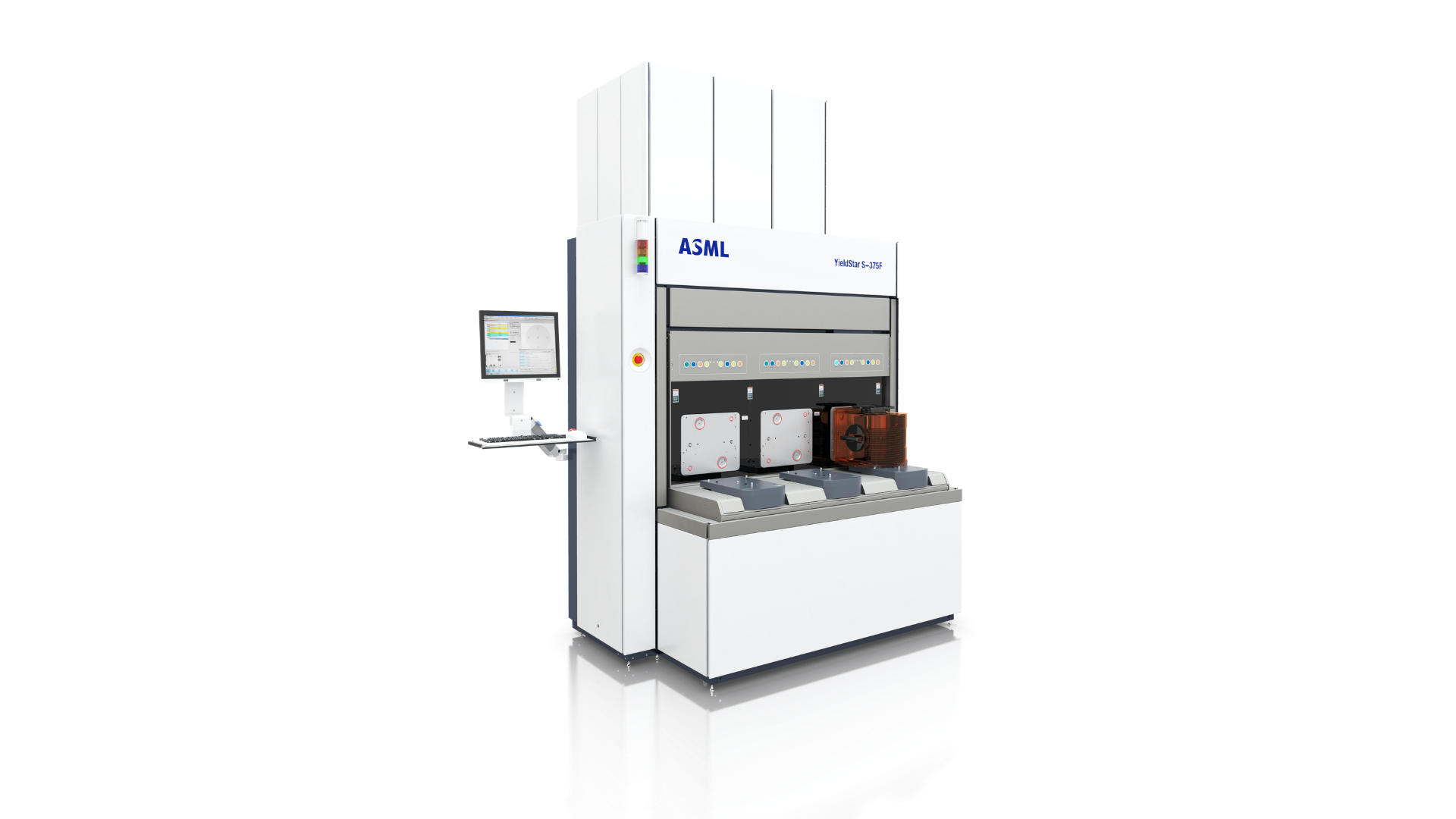
The YieldStar 1385 is a standalone optical wafer metrology system for post-etch overlay measurement of silicon wafers, allowing chipmakers to monitor the performance of their whole semiconductor manufacturing process.
The YieldStar 1385 is considerably faster than scanning electron microscope (SEM) solutions, reducing the cost of ownership for metrology. Novel data science techniques are used to extract in-device overlay measurements with nanometer-level accuracy. The in-device measurement capability allows for very high sampling densities which can enable advanced post-etch process control loops to improve overlay performance and yield.
The system can measure multiple layers at once, either through in-device chip features or small, dedicated metrology targets embedded in the chip design. Its fast measurement time allows chipmakers to measure more wafers, and more of the surface of each wafer, for better insight into production process performance. Advanced machine learning technology integrated into this system ensures accurate measurement while remaining insensitive to other stack variations for robust results under all conditions.