Electron optics is fundamental to ASML’s electron-beam (e-beam) systems. Chipmakers use ASML’s e-beam metrology and inspection systems to quickly and accurately measure chip pattern quality before and during high-volume production.
Working in electron optics at ASML
At our Silicon Valley location, people from many different professional backgrounds work together in collaborative, supportive teams to push e-beam technology to new limits. Here, physics experts can turn their passion for modeling into the next generation of semiconductor production technology.
In the engineering department we have three teams working in electron optics. The electron optics simulation team proposes and models innovative design concepts, meticulously tweaking their designs to meet tight performance constraints. The design team will implement the proposed models from the simulation team and turn them into real modules. After that the testing and integration team will integrate the modules, test and qualify the modules and support the system level integration. The three teams collaborate closely everyday to develop the advanced electron optics systems.
The team also works closely with other R&D departments to improve our systems’ performance by developing novel simulation tools for accurate modeling of a variety of critical scanning electron microscope (SEM) processes.

Electron optics in our technology
Our HMI e-beam metrology and inspection systems go hand in hand with our lithography systems to help chipmakers improve yield and produce faster, more powerful microchips.
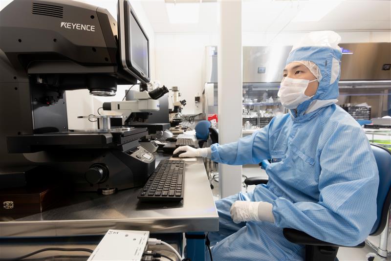
E-beam metrology and inspection systems are essentially scanning electron microscopes (SEMs) that can locate, image and analyze individual chip defects amid millions of tiny, printed patterns.
ASML’s multibeam inspection systems are the first machines to be able to split one electron beam into multiple beams to increase inspection throughput.

Career tracks in electron optics
Be an electron optics concept designer or mechanical designer, staying one step ahead of new development trends in e-beam metrology and inspection.
Use simulation tools to validate concepts, measure performance and support the testing and integration of our e-beam metrology and inspection systems.
Focus on performance improvement, feeding valuable data from scanning electron microscopes back to design teams.
Gain the opportunity to develop into leadership roles, including technical experts (‘architects’), project leaders and people managers.
See what our electron optics experts are saying
 Abhishek Vikram, Director of Product Management
 Xinan Luo, Technical Project Manager
 “Getting to collaborate with such innovative and creative individuals on this cutting edge technology is what allows us to deliver high quality solutions that are impacting the semiconductor industry.”
 Shuo Zhao, Principal Electron Optics Engineer
 From quantum theories to semiconductor realities
Delve into the intricate physics that underpin the development of cutting-edge semiconductor devices. Xiang Flora Li, shares her insights and experiences and a unique perspective on how quantum theories are transformed into practical semiconductor solutions.
.png?h=564&iar=0&w=1029)
Become a pioneer in this leading-edge field
Want to be alerted for new jobs?
Create job alert