Silicon Valley at a glance
ASML Silicon Valley, located in San Jose, develops sophisticated software and metrology solutions for chipmakers, enabling ASML’s holistic lithography approach.
Year acquired Brion
Year acquired HMI
Employees
2022 annual figures
Average employee tenure
2022 annual figures
Specialties
Find your passion at ASML Silicon Valley Electron optics
Read more
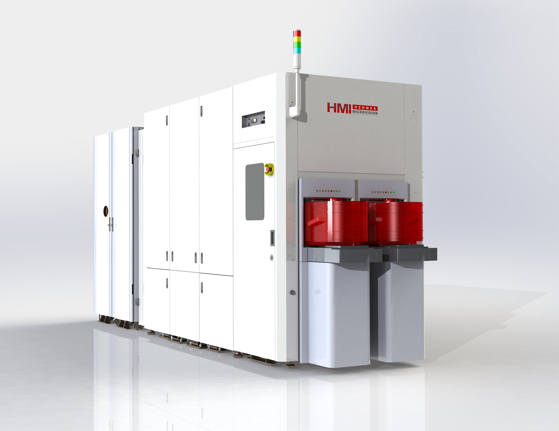
Design and build some of the most advanced electron-beam measurement tools in the semiconductor industry.
 Software engineering
Read more
Find out what it’s like working as a computer scientist or software developer at ASML working in C++, C#, Python or Java.
 Physics & Computer Science
Read more
Computer science and physics is at the heart of everything we do at ASML.
Our technology in Silicon Valley
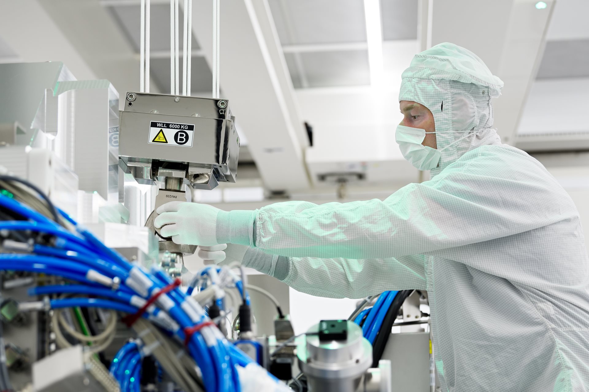
At ASML Silicon Valley, we develop sophisticated software and metrology solutions, addressing escalating complexities encountered at smaller nodes. Local customer support and technology development also ensure superior system performance and service.
Read more


Working and living in Silicon Valley
ASML Silicon Valley is located in San Jose, California – a dynamic area where technology and culture converge in a fast-paced, innovative environment. The third most populous city in California, San Jose ranks as one of the wealthiest cities in the United States.
Read more

Software heroines
Leading the way for women in ICT at ASML
Read about Mingjing Zhao, a senior software quality assurance manager at ASML in Silicon Valley, and other women as they pursue their dreams in computer science and software engineering at ASML.

ASML's Glassdoor rating
 Jinping Song, Head of HMI and Brion DevOps Team
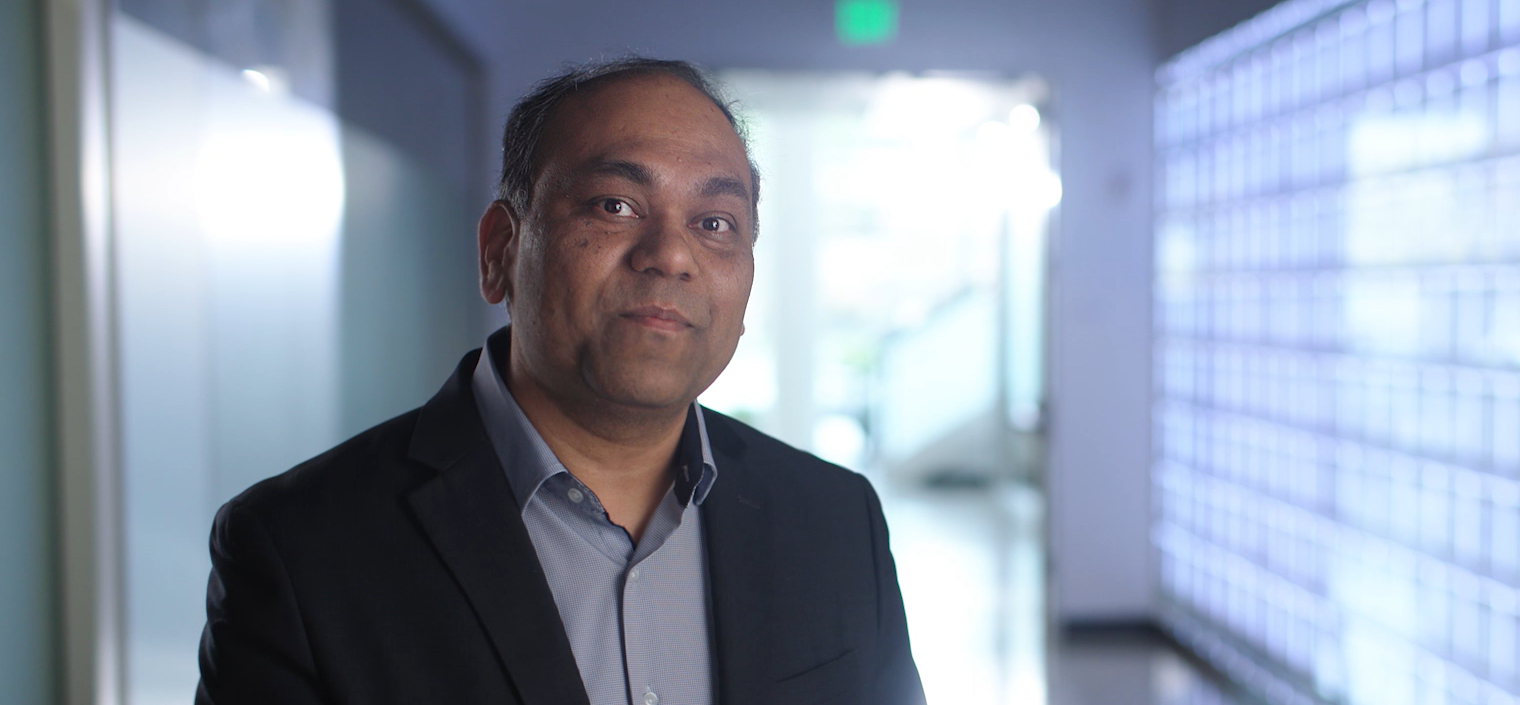 Abhishek Vikram, Director of Product Management
 "The Silicon Valley site works together with colleagues around the world to deliver a holistic solution to customers by providing our unique competency."
 Sheila Kang, Senior Software Engineer
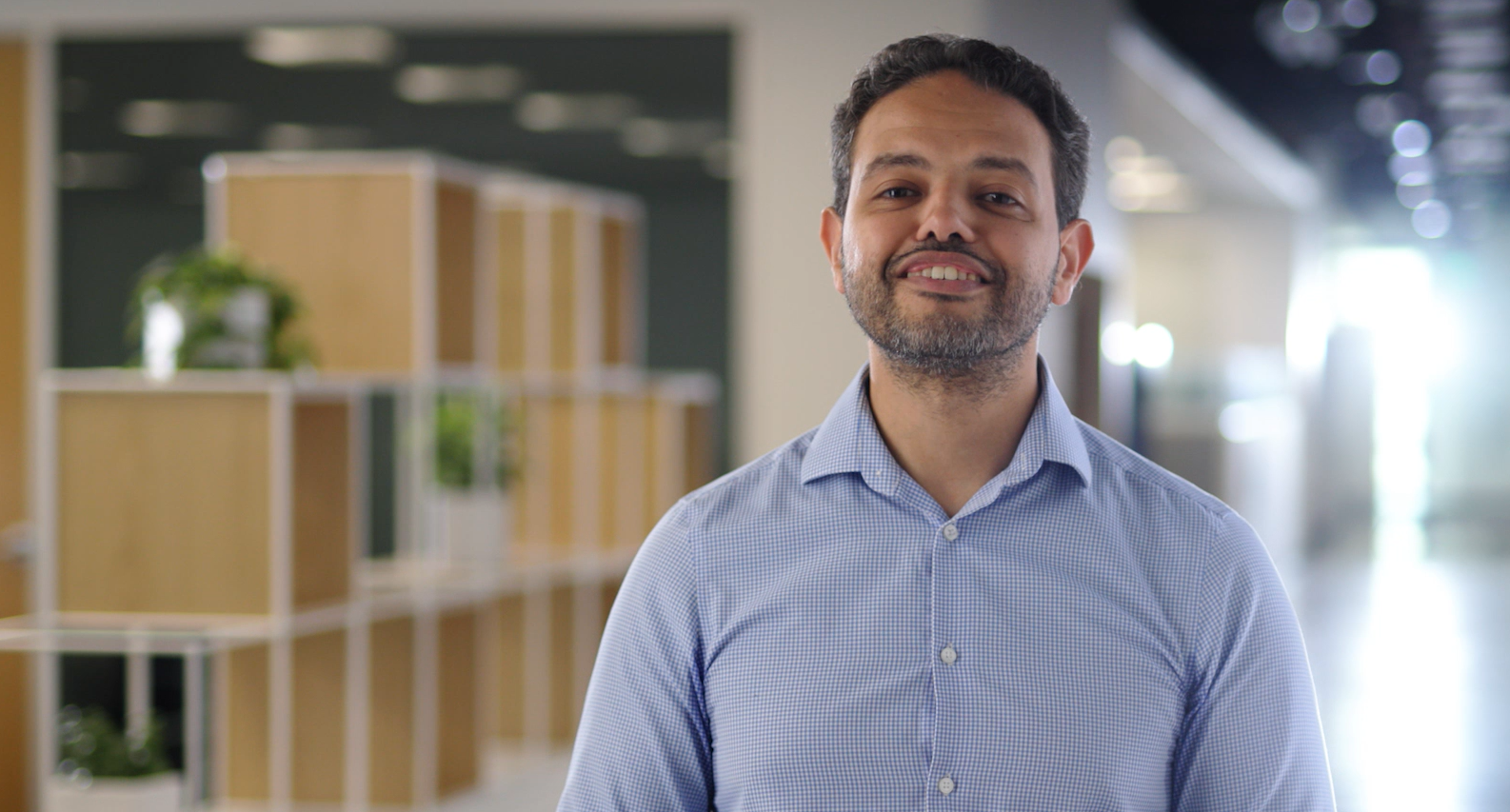 Mohamed Ali, Software Platform Engineering Manager
Discover what ASML has to offer in San Jose.
Want to be alerted for new jobs?
Create job alert