9-minute read - by Sander Hofman, March 30, 2022
Four decades, billions in R&D, a vital merger, thousands of people around the world: bringing EUV lithography to high-volume manufacturing was an immense effort. Learn about the pivotal moments that happened on the way to launching ASML’s first EUV system, as well as a glimpse of what’s next.
The dawn of EUV
The EUV story begins in the mid-1980s in Japan when, building on multilayer mirror research done in Russia in the 70s, Hiroo Kinoshita projected the first EUV images. Labs in the US and the Netherlands soon also began to explore this potential new development in lithography. Originally called ‘soft x-ray’ lithography, the name ‘extreme ultraviolet’ was inspired by the term used by astronomers for the same light wavelengths and photon energies.
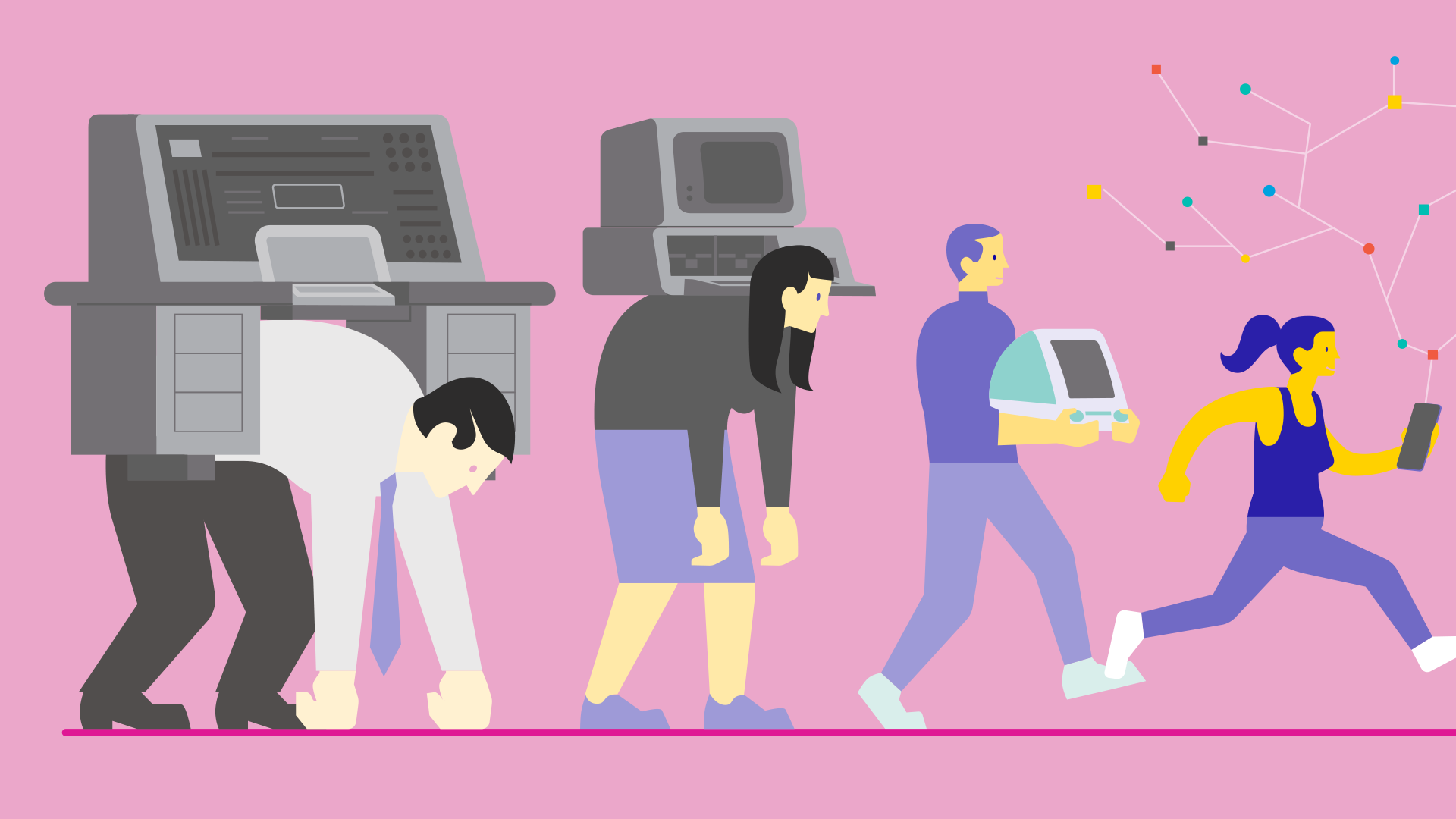
In lithography, using shorter light wavelengths enables chipmakers to shrink the size and increase the density of the features (or transistors) on a chip, making the chip faster and more powerful. When ASML was founded in 1984, the industry was using mercury-vapor lamps that produced light of 436 nanometers (nm), known as g-line, and later, ultraviolet (UV) light of 365 nm, called i-line. Early EUV researchers pursued several wavelengths ranging from 4 to 40, but eventually settled on 13.5 as the sweet spot for generating EUV light with tin plasma.
EUV wasn’t the only technology that researchers explored to enable future generations of ‘shrink’. Electron beam lithography and ion beam lithography seemed to be other viable options, but ASML placed an ‘educated bet’ on EUV lithography, because it was the technology that seemed best suited to continue transistor scaling while remaining affordable in mass production.
Not everyone was immediately sold on the idea of EUV technology, however. At a 2020 SPIE conference retrospective, Hiroo Kinoshita, who had then been a researcher at NTT, described the challenges of convincing his fellow scientists that EUV lithography had a chance. “[I presented my results] at the yearly meeting of the Japanese Society of Applied Optics in 1986,” he said. “Unfortunately, the audience was highly skeptical of my talk. However, my belief did not change.”
Andrew Hawryluk, long-time semiconductor industry veteran and then-researcher at the Lawrence Livermore National Laboratory, recalled similar frustrations at the conference. He explained how in December of 1987, a professor came to visit him and his team. After learning about their groundbreaking research in EUV, the professor asked, “But can you actually do anything useful with this stuff?”
“His words haunted me,” said Andrew, who went home for Christmas break and returned two weeks later with a 30-page whitepaper on EUV lithography. He and his team presented the paper at a conference later that year, but even then, finding support was difficult. “You can't imagine the negative reception I got at that presentation,” Andrew recalled. “Everybody in the audience was about to skewer me. I went home with my tail between my legs vowing never to talk about EUV lithography again.”
But a week later, Andrew got a call from William (Bill) Brinkman from Bell Labs, who subsequently succeeded in getting the US Department of Energy to fund national programs for EUV lithography research at Lawrence Livermore and Sandia Laboratories, in what came to be called the ‘Virtual National Laboratories’.
Toward industrialization
“Bill got us the money, but the money was going to run out sooner or later,” said Andrew. “What was absolutely critical was to get the industry involved to support this new technology.”
Andrew’s boss, the late Natale (Nat) Ceglio, was instrumental in recruiting companies to embrace EUV, including Intel.
The participating US chipmakers formed the ‘EUV LLC’, which contracted with the Virtual National Laboratories to accelerate EUV lithography development and reduce the risks associated with the industrialization of the new technology (EUV Lithography, Wurm, Stefan, Gwyn and Chuck, 2008).

Meanwhile, in the Netherlands, Fred Bijkerk, a professor of EUV optics, projected the first EUV images in the Netherlands in 1990. It wasn’t until the late 1990s, however, that research into the industrialization of EUV lithography began in Europe. In 1997, ASML brought in Jos Benschop (senior vice president of Technology) to kick off our EUV program.
With Jos’s help, in 1998, ASML formed a European industrial R&D consortium dubbed ‘EUCLIDES’ (Extreme UV Concept Lithography Development System) with our long-standing partner the German optics manufacturer ZEISS and synchrotron light source supplier Oxford Instruments. ASML also worked with other suppliers that included Philips Research and CFT, TNO-TPD, FOM-Rijnhuizen, PTB (the German national metrology institute) and Fraunhofer-IWS. ASML and EUCLIDES joined forces with the American EUV LLC in 1999, while Japan pursued EUV technology development through their ASET program (Association of Super-Advanced Electronics Technologies) and later the Japanese Extreme Ultraviolet Lithography Development Association (EUVA) program.
In 2000, Jos was able to present the EUCLIDES program’s first results at SPIE. Having seen what was possible, in 2001 ASML assigned a small group of people and modest resources to build a prototype EUV system.
The team achieved their goal in 2006, when the first EUV prototypes were shipped to imec in Belgium and SUNY (College of Nanoscale Science & Engineering) in Albany, New York. There, the prototypes were used to better understand EUV and how this new technology could fit into the semiconductor manufacturing process. Things were starting to get real.
Achieving ‘first light’
In the Spring of 2008, SUNY used their demo tool to produce the world’s first full-field EUV test chips. And in 2009, ASML opened the buildings that would house our 10,000 m2 cleanrooms and workspaces for EUV development and production at our headquarters in Veldhoven, the Netherlands.
Then, in 2010, we shipped the first TWINSCAN NXE:3100, a pre-production EUV system, to a Samsung research facility in South Korea. The machine achieved ‘first light’ (an astronomy reference) on Christmas Eve. For Jos, this was the culmination of 13 years of hard work.

“We started work on this in 1997,” he says. “Suddenly, it’s 2010, and you’re flying overseas to South Korea. You take a long taxi ride, change clothes, go to the fab [factory], turn the corner, and there it is: the machine. That is a great moment. What started as a dream became reality in a customer’s factory.”
It was a great moment, but it still took nine years before our customers began releasing products containing EUV technology. “The machine basics were there, but we struggled to achieve the productivity that our customers needed in order to make EUV an affordable choice,” Jos explains. “It’s important to remember that the R&D phase at our customers also takes time,” says Jos. “After EUV’s ‘launch’, it still took one or two nodes for chipmakers to mature the technology and learn how to use it fully before commercial products could be built with it.”
Part of the reason this process takes so long is that chipmakers have to optimize the infrastructure around the new technology. “Next to a scanner, you need to optimize things like the reticle and the photoresist, and the EDA (electronic design automation) – the software tools that you use to design a chip, making use of the full benefit of the new capabilities. It’s a constant feedback process, with data from each part of the process influencing the others,” Jos explains.
In 2012, our key customers Intel, Samsung and TSMC agreed to contribute to our EUV R&D over a period of five years as part of our Customer Co-Investment Program, acquiring stakes in the company in return. We shipped six more systems to different customers in Asia and the US, and in 2013, we shipped the first EUV production system – the TWINSCAN NXE:3300 – signaling another step forward in the development of this new technology.
Technology challenges along the way
“It took longer and was much more work than I imagined,” says Jos, looking back on the process. “You could say that we were either brilliant or just stubborn,” he laughs.
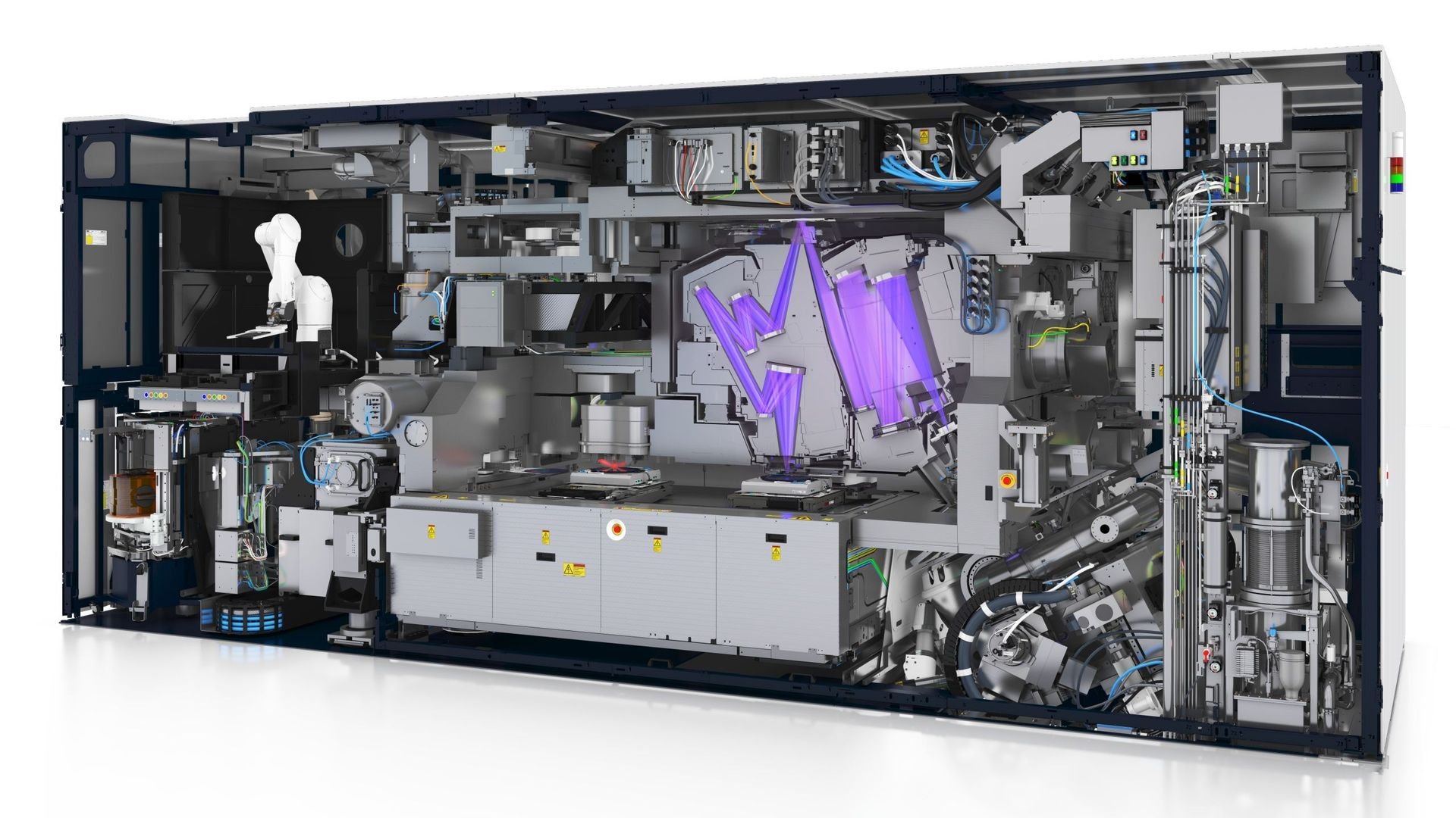
To make the jump to extreme ultraviolet light of 13.5 nm required innovations in practically all areas of the lithography machine, including the light source, the optics that shrink and focus the light onto the silicon wafer, and the reticle containing the blueprint of the chip to be printed. To make matters more complicated, EUV light is absorbed by almost everything, so it has to be produced and used inside a high vacuum environment. “The whole switch to vacuum was quite an adventure,” Jos recalls. “It made the materials a challenge due to outgassing – what materials you could use and how you had to handle them and clean them.”
“Our research really gained traction when ZEISS showed it could make specialized EUV optics,” explains Jos. Optics had always been the biggest anticipated challenge for EUV, but thanks to ZEISS, it quickly dropped off the list of critical issues.
ASML’s focus then shifted to solving the ‘source’ challenge. “We got a lot of public beating because of the source,” Jos admits. “Multiple customers would refer to our source roadmap and say, this is what you promised years ago, and the reality is nowhere near it. They practically crucified us at SPIE.”
In the early 2000s, ASML had started collaborating with several potential suppliers for the EUV source in the Netherlands, Japan and the US, including San-Diego-based Cymer. ASML chose to go with Cymer’s solution, later acquiring the company in 2013. But the R&D was much harder than anticipated. Designing the laser-produced plasma (LPP) source involved hitting droplets of tin 50,000 times per second – twice – to vaporize them, creating a plasma 40 times hotter than the surface of the sun to emit EUV light.
“We actually had some early success, and things looked pretty promising, and we thought maybe this is not as hard as we expected!” says Danny Brown (head of EUV Source System Engineering & Research). “And boy, we were wrong.” The main challenge was achieving 250 W of power in a full-scale demonstration source vessel. Despite many setbacks, the team working on it eventually succeeded and went on to receive the Berthold Leibinger Innovation Prize in September, 2021.

EUV is here to stay
After we reached 250 W in the source (which enabled a factory throughput of 125 wafers per hour) and industrialized it, the end of the tunnel was in sight. According to Jos, the point at which we finally felt like our EUV program had succeeded was in 2018, when our customers began to invest heavily in the new technology in their fabs. “They were spending billions building fabs and buying our machines, which showed that they really believed in EUV.”
In 2019, the first EUV-enabled commercial product was released (Samsung’s Galaxy Note10 and Galaxy Note10+ smartphones). In December 2020, ASML celebrated the 100th shipment of an EUV system, and as of the end of 2021, 127 latest-generation EUV machines were in use at customer locations around the world. “It took a long time, but EUV is taking over the critical layers for Logic as well as DRAM Memory,” explains Jos. “The best moment in my career was in 2019 when I spoke at a workshop – I got my Samsung smartphone out and said, ‘I once said naively that EUV would be in volume production in 2006. I shamefully admit that it's 13 years late,’ but then I waved my phone and said, ‘but some of you thought this thing would never exist.’”

What’s next? EUV 0.55 (High-NA) and beyond
In our quest to enable ever-smaller chip features, we continue to innovate and are now increasing our EUV machines’ numerical aperture (NA) from 0.33 to 0.55, which means that the optics in the new systems will allow light with larger angles of incidence to hit the wafer, giving the system a higher resolution and decreasing the size of the features that can be printed. “Because this new lens is fundamentally different, it meant that we had to come up with a completely new way of manufacturing it and measuring its features,” explains Jos. “Our teams at ZEISS and in Wilton are breaking one world record after another.” The first shipments of EUV 0.55 ‘EXE’ machines to customers for R&D purposes are planned for the end of 2023, and we expect them to be used in high-volume manufacturing in 2025.
But in 2022, our biggest challenge is ramping up production of EUV systems from 40 to around 60 systems per year. Hiring more people and building more cleanroom space are only part of the problem – the crux of the difficulty lies in ramping up capacity in our supplier network to meet the demand for EUV machines, according to Sheila Leenders, vice president of our EUV Factory. “Our supply base is facing the challenge of a lifetime,” she says. “We’re working hard to help them increase capacity and improve reliability where it’s needed at our suppliers around the world.”
Overcoming challenges through collaboration
Over the years, ASML pushed through many setbacks, unexpected challenges and delays. But Jos says that whenever they saw a new challenge looming, they always had ideas for how to tackle it. “Through our network of trusted partners, we always found ways to solve it,” Jos says.
“The way we approach any technology is by working through collaborative networks,” he continues. “This allows us to make use of the knowledge available and to progress with an ‘acceptable’ risk profile.”
Throughout all phases of EUV technology development – research, industrialization and now high-volume manufacturing – working together across borders has been key. Today, we procure some critical EUV modules from the US, such as the droplet generator for the light source as well as sensors, reticle handlers and stages, and other modules from Germany, such as our ZEISS optics and TRUMPF’s lasers for the EUV source, and we collaborate with companies and institutions all over the world in continued R&D for the next generation of EUV machines. Acting as the system architect at the center of things, ASML succeeded in building and mobilizing a global ecosystem to industrialize what many considered to be impossible technology. And we’re now confidently taking it into high-volume manufacturing.
Want to discover more about EUV at ASML?