7-minute read - by Sander Hofman, August 2, 2023
After more than 70 years of relentless innovation to produce smaller, better and cheaper chips, the world’s most advanced chipmakers are currently getting ready to mass produce chips on the 3-nanometer process node. But did you know that the industry’s ability to make ever-finer circuitry on silicon almost got stopped short at the 65-nanometer threshold – if it weren’t for a puddle of water? Read on to discover the inspiring history behind our immersion DUV lithography systems.
The risk of shrink
In the early 2000s, the chip industry had been working on a transition from lithography with argon fluoride (ArF) light sources at 193 nanometer to lithography with fluorine (F2) light sources at 157 nanometer. Like an artist wishing to draw a more precise, detailed picture by replacing a marker with a fineliner pen, this significant shift to a smaller wavelength was the industry’s hope to continue shrinking transistors and enable more computing power as well as memory function on a chip. However, in an unexpected turn of events demonstrating the risk of pushing engineering to its limits, the laws of physics disagreed.
As the engineering came together for the first 157-nanometer lithography systems, adopting calcium fluoride lenses as the new type of optics in these systems was considered challenging yet feasible. However, imaging experiments on actual prototype lithography systems revealed significant double refraction effects. What’s worse, the effect was inherent to calcium fluoride and far exceeded the imaging specifications. The chip industry hit a wall as the obvious roadmap for lithography seemed to have come to a grinding halt.
A puddle of water, a twist of fate
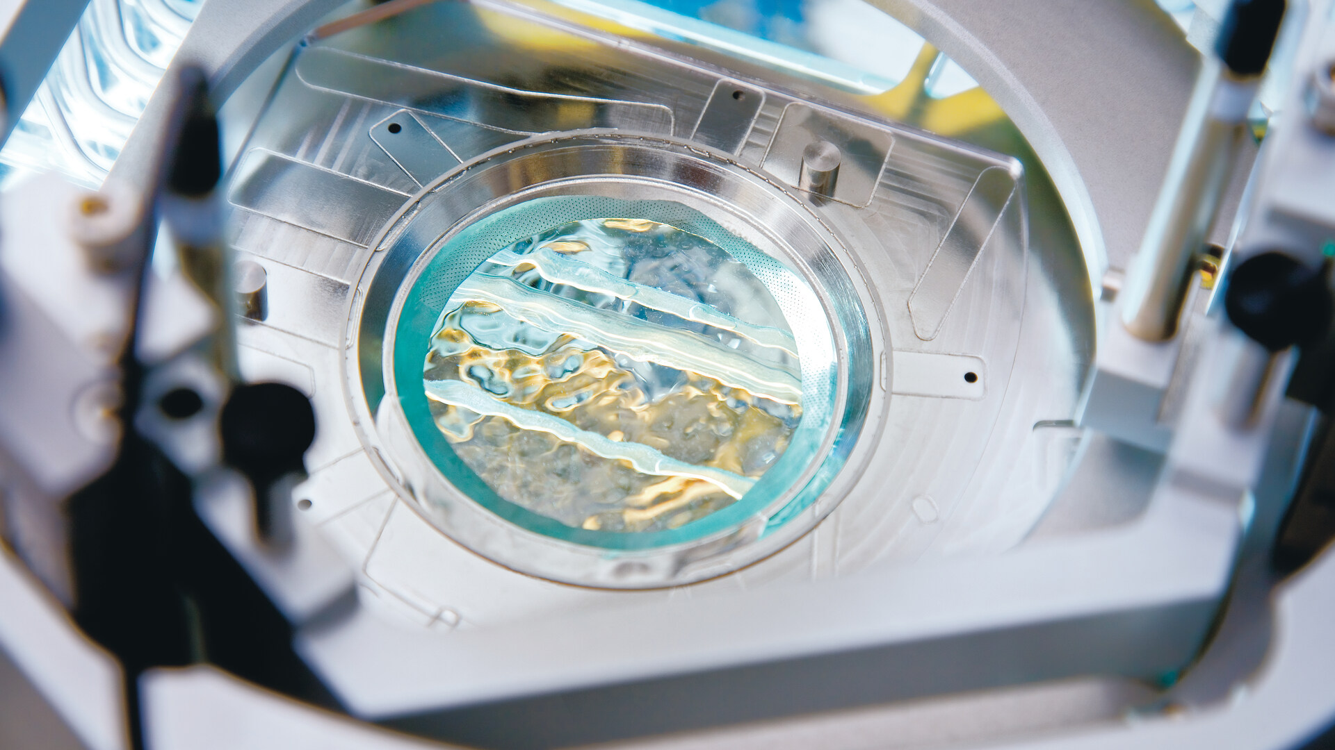
In December 2001, ASML researcher Jan Mulkens (now an ASML Fellow) attended an industry conference on 157-nanometer lithography in the United States where industry professionals came together to identify potential next steps. Their discussion honed in on adding a layer of purified water under the lens to sharpen the resolution, an optical phenomenon first discovered and harnessed by microscope pioneers Robert Hooke and Antoni van Leeuwenhoek, and first described for use in lithography by IBM in the 1980s. Jan and his colleagues realized that this optical technique could extend 193-nanometer lithography further, bypassing the industry's burning challenge of trying to fix 157-nanometer lithography. Furthermore, by using water as the optical fluid, all of the existing optics, masks and photoresists could continue to be used. This was the best chance to keep Moore’s Law going.
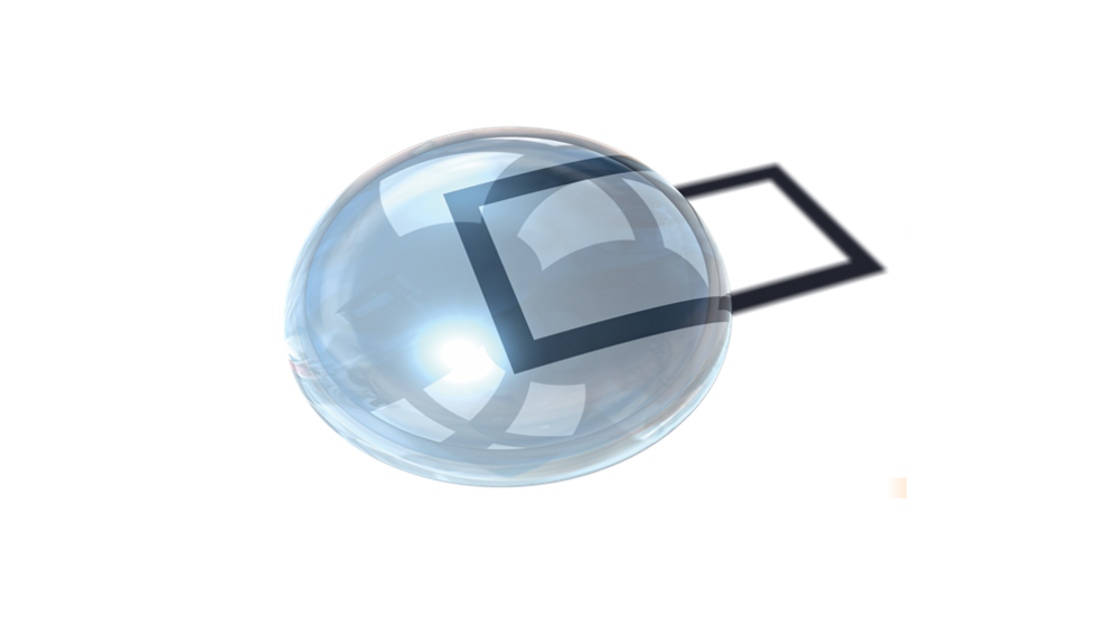
“Projecting light through highly purified water would allow significantly smaller chip features to be printed, because the liquid allows the design of an optical lens that more accurately images the fine patterns on the wafer,” explains Jan. “But when we first started thinking about using this principle in a lithography machine, people found it odd. Water was associated with splashes, droplets and bubbles – would that really work in a complex and highly accurate imaging system?” Introducing water into the system that might not flow safely and securely through a hose appeared to be an impossible task.
Upon returning to the ASML headquarters in Veldhoven, the Netherlands, Jan gathered a small team, convinced that competitors would soon follow suit. If they wished to seize this opportunity, they would have to act quickly. With a heightened sense of urgency, Jan’s team started by defining and testing some of the basic immersion concepts. “When we showed the basic feasibility of immersion lithography through a series of experiments and conceptual ideas for the system architecture, we got the green light to scale our concept to a full-size prototype system with a team of 20 colleagues,” Jan recalls.
Three advantages that sped up ASML’s immersion program
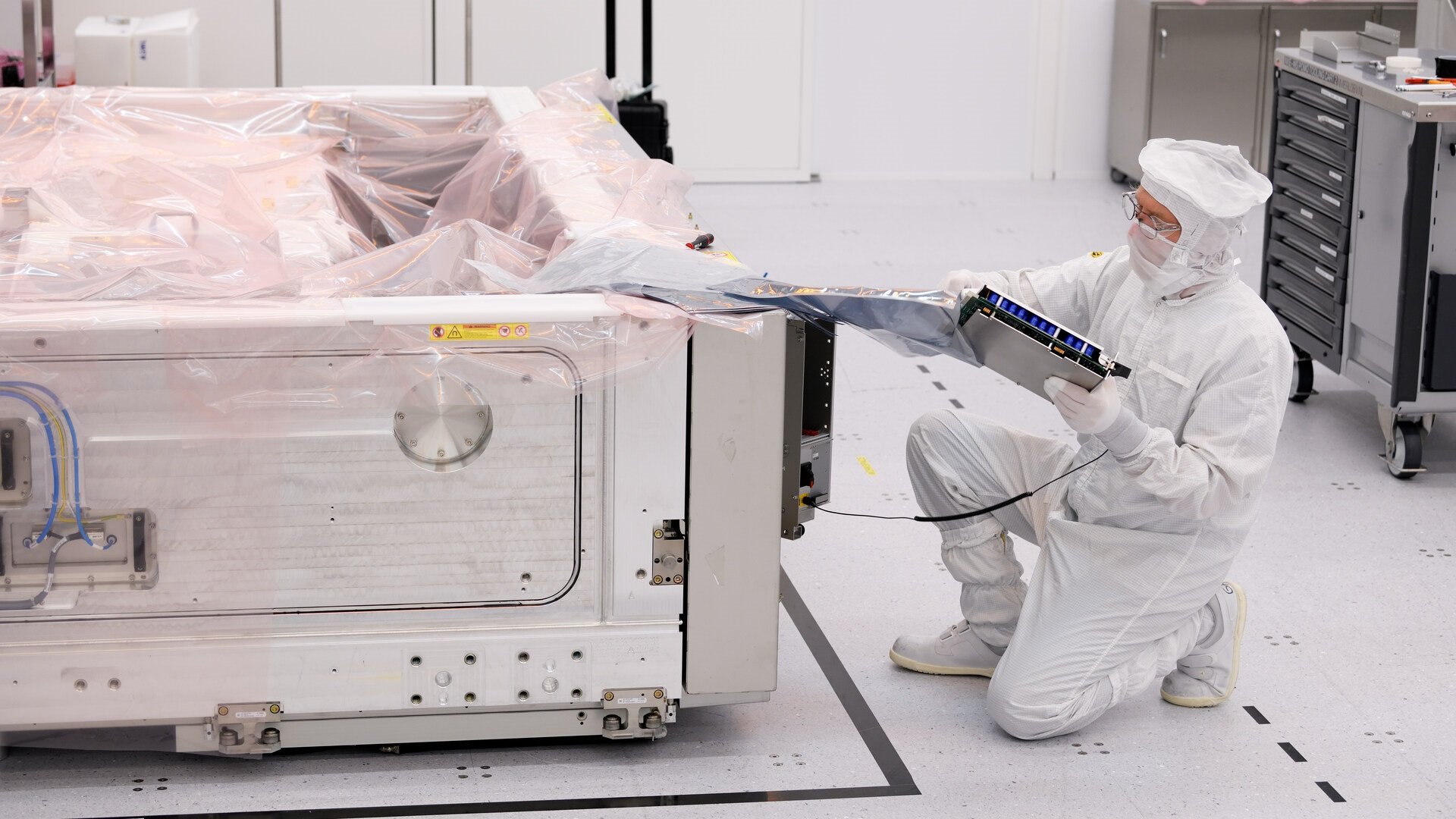
The team made quick progress thanks to the TWINSCAN platform. Our systems were able to do two things at once thanks to the proprietary dual-stage architecture: one stage measured the wafer position for accurate alignment and focus, while the other stage moved precisely under the lens to image the pattern on the wafer. Jan's team realized as they sketched out the dual-stage architecture of an immersion system that chipmakers could leverage the resolution enhancements of immersion lithography on one stage while continuing with our tried-and-true dry metrology on the other, achieving a win-win.
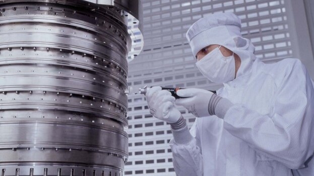
Another advantage we had was our close collaboration with ZEISS. In parallel to the adoption of the Veldhoven system architecture, ZEISS optics design engineers in Oberkochen, Germany, figured out how to slightly modify a regular lens so that it could be used in immersion lithography. As a result, chipmakers saw an opportunity to quickly test early immersion systems in their pilot fabs while preparing for high-volume chip manufacturing with the new technology.
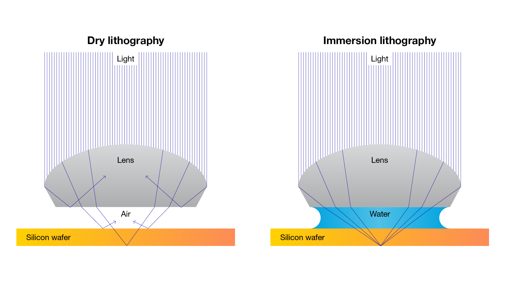
Finally, our ecosystem provided another benefit: long-time research partner Philips Research had developed a high-density optical recording technology that utilized an immersion lens. Their research and engineering expertise were put to use in developing the technical concept for a lithography system that could move and hold water under the lens.
By autumn 2003, the immersion team was able to demonstrate concrete imaging results on the ASML prototype system dubbed the TWINSCAN AT:1150i. "The proto results changed the lithography roadmap almost instantly," Jan says. "We defined a series of new lithography systems in a very short period of time that would directly address the chip industry's resolution struggle."
In December of the same year, we publicly announced the industry’s first immersion lithography system, the TWINSCAN XT:1250i. This pre-production system combined the enhanced resolution and depth of focus of immersion lithography with the precision of dry lithography on the XT, a much more compact platform.
Controlling the pesky puddle
While we were able to achieve tremendous progress, immersion lithography was not out of the woods yet. It had to now be prepared for mass production. Defectivity posed a real threat to the economics of early immersion systems as any flaws in reproducing the geometric pattern of the mask onto the silicon wafer would result in yield loss, which was the most important performance indicator in a chipmaker’s mass production process. Adding a puddle of water to a high-speed stage introduced two new potential sources of defects: bubbles could form under the lens, degrading imaging performance. To make matters worse, escaped water droplets could interact uncontrollably with the photosensitive coating on the wafer. It was not an option to sacrifice system productivity by slowing down the wafer stage: doing so would make the system unaffordable.
To better understand the behavior of the puddle and find ways to control it, researchers at ASML again tapped into our extensive academic network. Professor Detlef Lohse, a German fluid dynamics and mechanics researcher at Twente University, dedicated considerable time and energy to furthering our knowledge about the fundamental physics at work in immersion lithography. This improved understanding sparked engineering ideas from our Research and Development team and high-tech supply chain. The team narrowed the solution space enough to identify a basic engineering mechanism: dubbed the 'immersion hood,' this new part of the lithography system formed a ring around the last lens element to control the puddle. "Over the years that followed, basic prototypes could be tested, the best concept would be industrialized, and this ultimately allowed us to triple the speed of the wafer while reducing defectivity by an order of magnitude," says Jos Benschop, Senior Vice President of Technology at ASML. By the end of 2004, TSMC had announced the first fully functional 90-nanometer node chips manufactured with our early immersion systems.
By 2006, we had launched XT:1700Fi, bringing immersion lithography into volume production. The numerical aperture of the new system increased from 0.93 to 1.2, bypassing the perceived pre-immersion barrier of 1.0 and providing a viable path to continue shrinking transistors past the 65-nanometer node. The system's record-breaking imaging performance enabled chipmakers to improve resolution by 30%, the largest improvement in decades, while system productivity increased to 122 wafers per hour, also a record at the time.
Further refinements and new systems followed, driving up imaging performance and system productivity while allowing chip makers to catch up with Moore's Law and push their roadmaps forward.
Multi-patterning and the ultimate immersion platform
While immersion lithography resulted in significant resolution gains, Moore's Law continued unabated. Chipmakers soon realized that even sharper imaging was required to realize their roadmaps to the 32-nanometer node and beyond. Chipmakers began experimenting with various types of multi-patterning technology, which exposed multiple simpler, interlaced patterns to create one complex layer pattern.
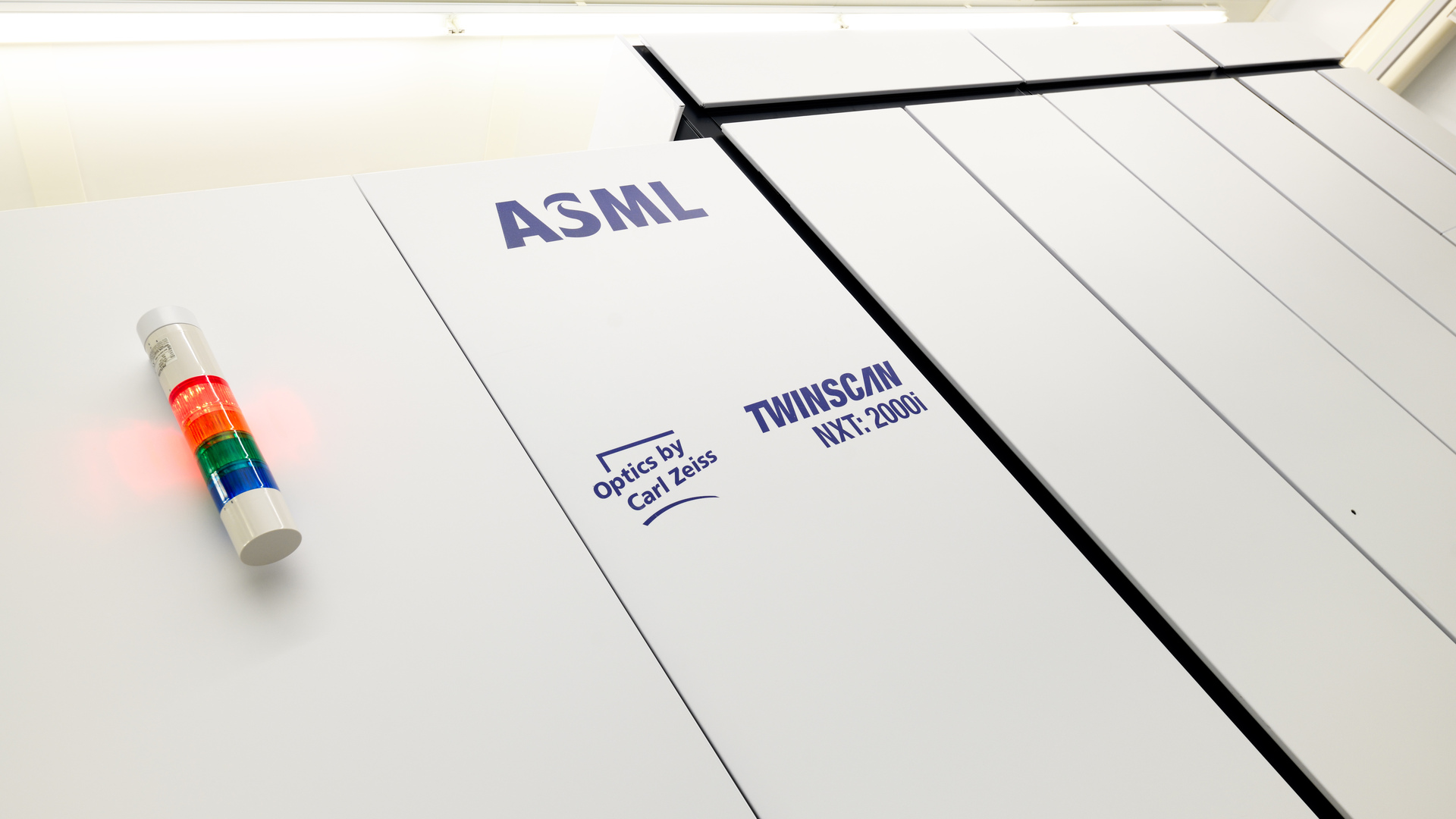
"Multi-patterning was a fundamental change for lithography," comments Jos. “Suddenly, overlay, rather than imaging resolution, became the critical parameter for enabling shrink. The additional costs of multi-patterning made it critical to increase the productivity of immersion systems in order to keep shrink cost-effective." This is why we began developing the NXT platform, the successor to the compact XT platform. Using magnetically levitated wafer stages and a position measurement system based on encoders instead of interferometers, the platform enabled much more precise positioning of the stages at higher speeds as well as faster stage swapping. In an industry where time is money, our ability to combine the speed of the NXT platform with the resolution of immersion lithography ensured that the market share of the NXT platform could continue to grow. The TWINSCAN NXT:1950i was introduced in 2008 for use in mass production of the 32-nanometer node, and it quickly inspired the development of a series of systems for use in sub-32-nanometer nodes, including the NXT:1960i, NXT:1965i, NXT:1970i and NXT:1980i.
Immersion lithography continues to drive innovation
Currently, the NXT platform accounts for approximately 80% of the more than 1,100 immersion systems shipped to date. Immersion system market demand is at an all-time high and is expected to remain strong beyond 2023. Our most recent NXT immersion scanner, the NXT:2100i, which was released at the end of last year, demonstrates our engineers' unwavering commitment to pushing this technology forward. It has next-generation imaging capabilities thanks to a lens-adjustment system and is currently used in the most advanced chip nodes at leading chipmakers worldwide. Overall, the productivity of NXT immersion systems has more than doubled in the last nine years, with the most recent systems capable of running more than 6,000 wafers per day. This translates into good value for money for chipmakers.
It’s no exaggeration to say that to remain competitive in the semiconductor landscape, companies need to understand and respond to the industry's unique challenge of addressing technological complexity while ensuring manufacturing affordability. This has been a fundamental approach that has always guided our efforts in bringing immersion lithography to fruition, and while the technology's challenges have evolved over time, our focus on immersion's productivity and affordability for chipmakers as well as the industry as a whole will stay unchanged.
Learn more about our immersion DUV systems. Want to join us as an engineer at ASML? Check out our latest R&D jobs.
