5-minute read - by Jessica Timings, August 18, 2021
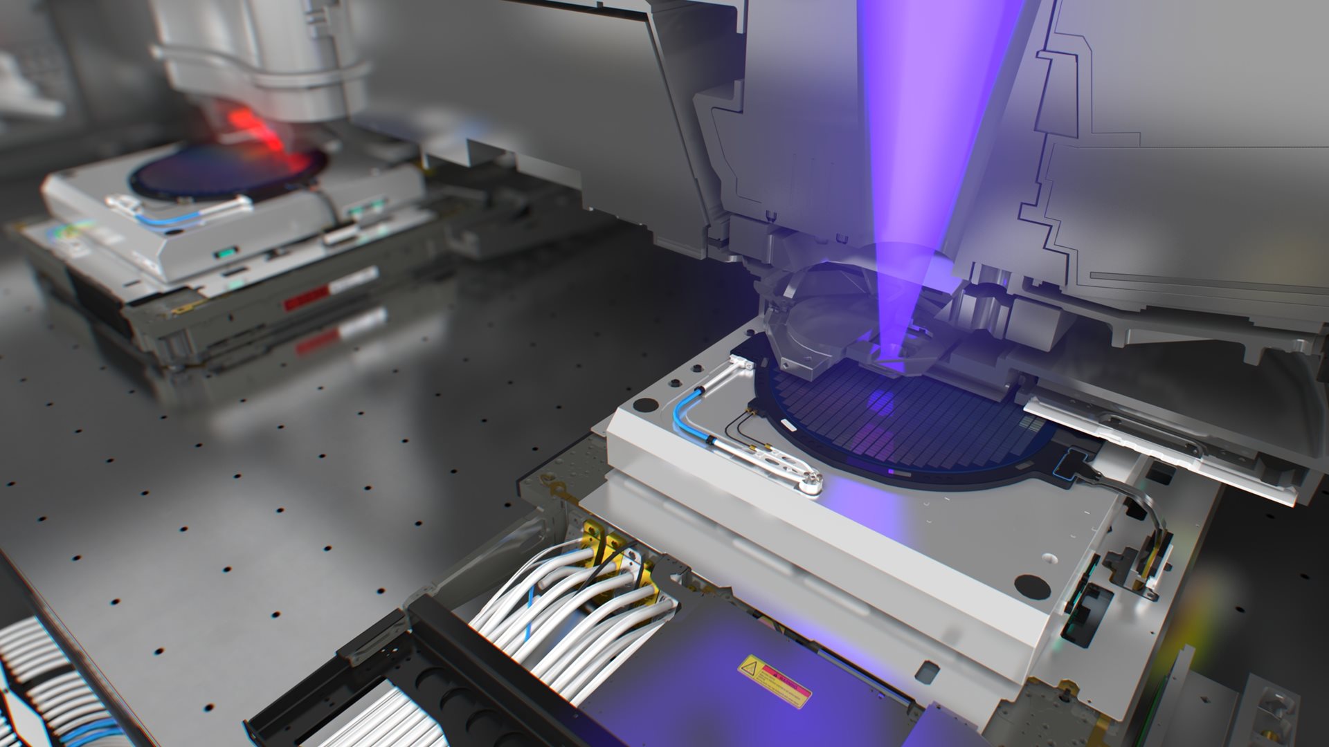
In mid-2020, at the height of the COVID-19 pandemic, ASML shipped its first-ever dry NXT system. It was the first lithography system of any kind capable of processing more than 300 wafers per hour. But it’s the history of TWINSCAN – the platform on which these systems were built – that is most fascinating.
ASML came of age as a lithography supplier with the PAS 5500 platform in the early 1990s. Around the same time, precision mechanics and interferometer expert Bert van der Pasch was working on the interferometer systems and wafer handler of the PAS platform. He had started his career at Philips, where his technological knowledge had been fostered.
"Without Philips, ASML wouldn't exist," says Bert. "But what I liked about ASML was working on real products and their problems.
"For example, when I was working on the scanner, at one point there were seven dynamical shortcut issues. Normally, you investigate one and change if required. A normal person would do that, but not ASML. We decided to change all seven at once – and it worked! We never knew which one did the job, but the problems were all gone."

Bert and the team’s continual innovation kept the PAS 5500 ahead of the game, delivering what was at that time industry-leading productivity and resolution. But with the new millennium approaching, ASML realized it needed a revolutionary innovative approach to give its customers the next leap forward in productivity.
Like many breakthroughs, the solution seems simple in hindsight. Wafers must be precisely scanned before the pattern is exposed onto them. Both the scanning and the exposure take time, and previous gains had come from reducing the time for each process. To save even more time, why not scan one wafer while the one before it was still being exposed?
A new stage for lithography
"It was limited new technology, but what was a revolution about the TWINSCAN was the swapping of the stages," says Bert. "Lots of things were normal developments, but that chuck swap was different. We just had to make it work."
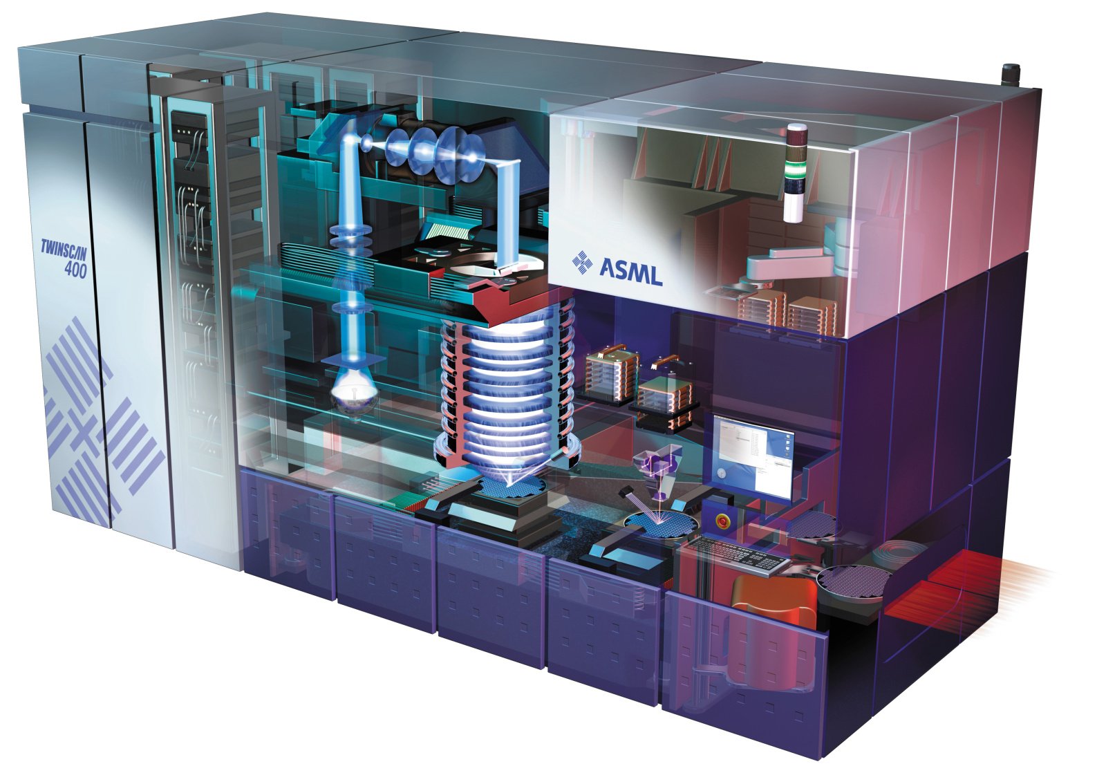
And thus, the TWINSCAN platform was born. TWINSCAN was the first – and is still the only – lithography system platform with two complete wafer table modules (or wafer stages). Wafers are loaded onto the wafer table modules alternately. When the wafer on table one is being exposed, another wafer is loaded on table two and then aligned and mapped. The tables then swap position so that the wafer on table two is exposed while the wafer on table one is unloaded. A new wafer is then loaded, aligned and mapped.
The first TWINSCAN system with this revolutionary dual-stage technology was shipped in 2001. The TWINSCAN AT:750T was a KrF lithography system, using light with a wavelength of 248 nm and targeted production at the 130 nm node. It was soon joined by an i-line system, the TWINSCAN AT:400T, and an ArF system, the TWINSCAN AT:1100, to span the range of lithography technologies then in use and enable all chip layers to be exposed on the new platform.
As with the earlier PAS 5500 platform, ASML's continual innovation provided incremental improvements to the resolution, precision and productivity of the TWINSCAN platform – delivered as changes to the basic platform, new systems and in-field upgrades.
The first such TWINSCAN evolution came in 2004 with the switch from the AT system to the XT system. XT systems were 25% smaller than their AT equivalents yet delivered the same or better performance. This allowed chipmakers to produce more chips from the same factory floorspace.
Just add water
Later that same year, ASML introduced its first immersion lithography system: the TWINSCAN AT:1150i. Immersion lithography uses a pool of ultra-pure water between the lens and the wafer to increase the lens's numerical aperture (NA) – a measure of its ability to collect and focus light. With conventional 'dry' lithography, NA can only reach about 0.93. Immersion made it possible to create systems with an NA up to 1.35.
"Immersion was a revolution," says Bert. "This was a thing that you can say in the beginning – will this work?"
Higher NA allowed systems to deliver better resolution and depth of focus with the same wavelength of light and resolution, making it easier to manufacture layers with smaller features. This, in turn, paved the way for modern technologies such as touchscreen and Bluetooth, as well as enabled the rise of mobile laptops over PCs.
Seeing double with NXT
Over the course of the 2000s, chipmakers started to reach the resolution limit of traditional lithography using immersion ArF systems. Yet the constant drive for new, more advanced chips meant they needed to be able to print even smaller features. ASML had started to explore a new extreme ultraviolet (EUV) light source – one that would enable patterning at unimaginably tiny scales. But progress was slow and challenging, and the demand from chipmakers to shrink was not going away.
So, in the meantime, the industry began exploring an approach known as 'double patterning' (also called 'multiple patterning'), which involves splitting one complex layer pattern into two (or more) simpler patterns that can be exposed separately to print the original pattern.
As its name suggests, double patterning requires twice as many exposure steps and the ability to align two patterns extremely closely. To make it feasible and cost-effective, lithography systems had to become significantly faster and more precise. The result was the next major TWINSCAN evolution: the NXT platform, which featured completely reengineered and significantly lighter wafer stages.
Just like in the days working on the PAS 5500 platform, the pressure from customers was on – and so ASML chose a revolutionary approach.
"We developed the NXT in parallel with the next-generation system for the new EUV light source," Bert explains.
The first NXT system, the TWINSCAN NXT:1950i, was launched in 2008 and delivered a 30% increase in productivity to over 200 wafers per hour, while also improving overlay to 2.5 nanometers (nm). Today’s leading NXT immersion systems can process 295 wafers per hour with overlay down to 1 nm.
Becoming extreme
Historically, the big leaps forward in the resolution of lithography systems have come from changing the wavelength of light used. Immersion and multiple patterning bucked this trend for a while, allowing chipmakers to maintain their roadmaps for creating ever more advanced chips with smaller features and while transitioning to many new technology nodes using familiar ArF lithography.
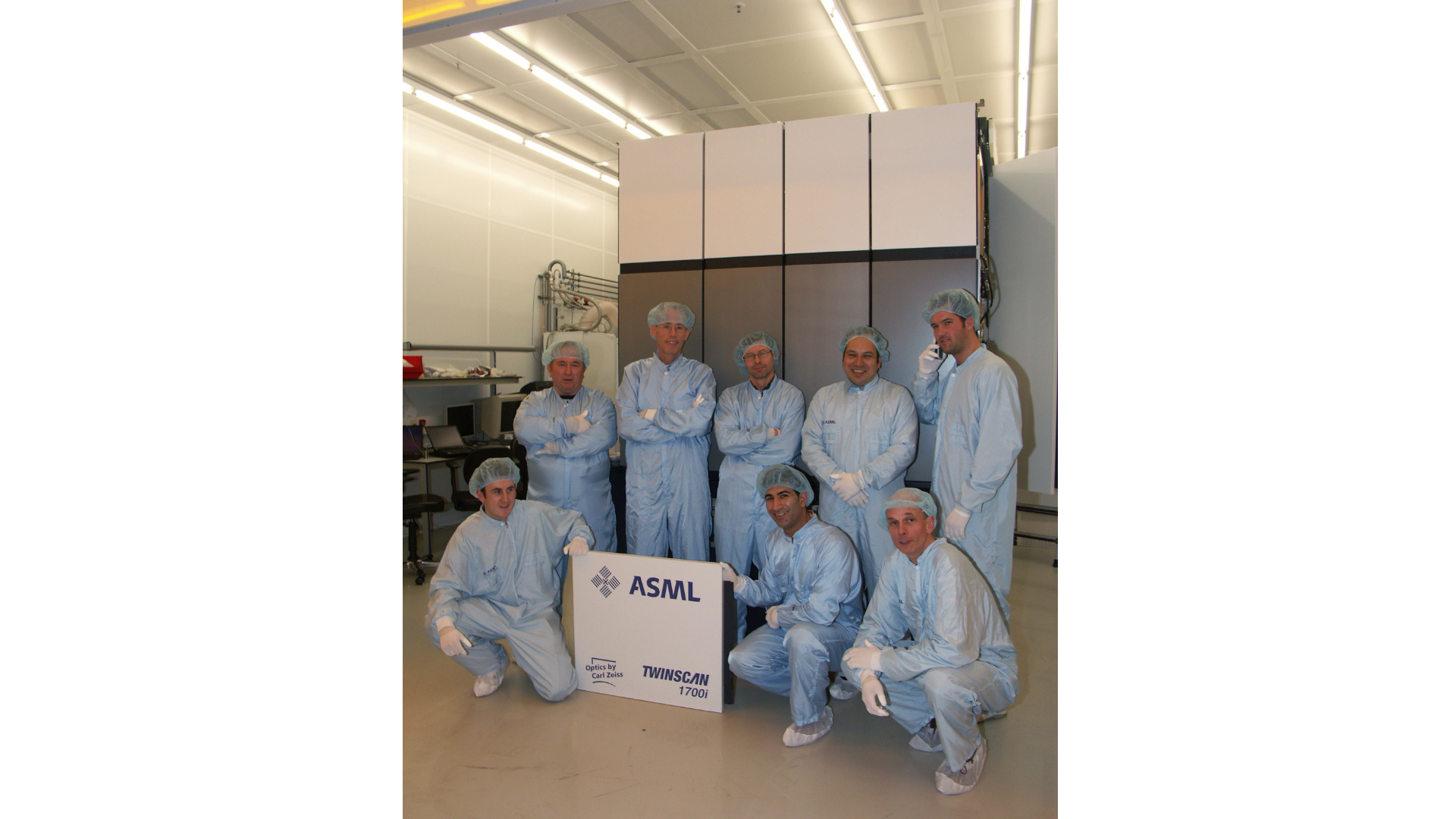
After 20 years of intense research and development, ASML succeeded in developing a new light source for a lithography system using EUV light with a wavelength of 13.5 nm. Light at this wavelength is absorbed by almost all materials, so these systems would need to maintain a high vacuum for the entire light path. This requirement led to the next generation of TWINSCAN: the NXE platform. The first prototypes of NXE systems were shipped in 2006 to help chipmakers start to learn learning about the brand-new technology. By 2016, chipmakers began ordering our first production-ready EUV system: the TWINSCAN NXE:3400.
A dry runner
Understandably, lithography technology innovation tends to be focused on the cutting edge – creating new systems for critical layers of chips with ever smaller features.
However, critical layers and cutting-edge lithography systems account for only one or two of the hundred or so layers that make up a modern chip. The bulk of chipmaking involves larger features exposed using mature lithography technologies. For these layers, value mainly comes from speed, and the fastest lithography systems use the TWINSCAN NXT platform. With the emergence of EUV in volume production of critical layers and immersion NXT systems being increasingly used in next-to-critical layers, ASML decided to extend the NXT platform to 'dry' technologies for use in sub-critical layers. This resulted in the TWINSCAN NXT:1470 – the first dry system to achieve on-product overlay better than 4.5 nm. It became the first lithography machine of any kind capable of processing more than 300 wafers per hour.
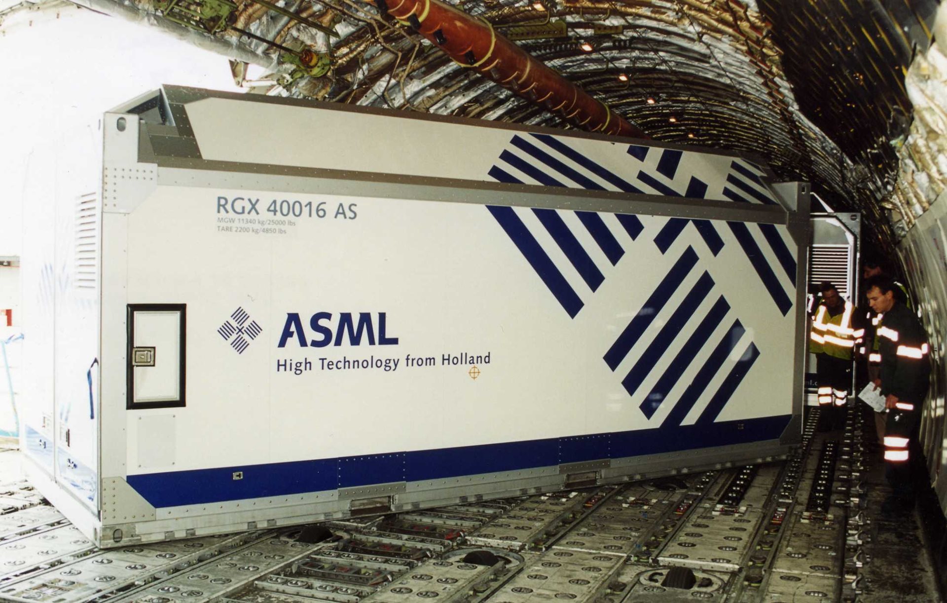
As the TWINSCAN dual-stage platform gets ready to celebrate its 20th birthday as a commercial technology, it has already evolved significantly to meet the varied challenges the semiconductor industry has faced. In 2021, we celebrated the 100th refurbished TWINSCAN, demonstrating our commitment to the circular economy. As the industry's leading lithography platform, TWINSCAN's ongoing evolution will continue to help chipmakers improve performance and reduce the overall cost of chip production.
"The market will continue to want us to perform better and better and produce better and better products," says Bert. "Thankfully, our employees have the same mentality that I recall from the 1990s and up until now: energy and commitment to finish something, to optimize it, to make it work. It's the culture of ASML, but also it comes with the pride of work for this company."
