3-minute read - by Peter van den Hurk, December 22, 2021
Microchips are made up of layer upon layer of patterns. To ensure the microchip works, the patterns in different layers have to line up with extreme accuracy. New ASML Fellow Simon Mathijssen explains how he and his colleagues are working to make that possible.
Lithography systems print patterns onto wafers. As many as 100 of these patterns are needed to make a microchip – and they all have to align with each other precisely for the chip to work. A lithography system’s ability to line up one pattern with the previous one is measured by its overlay performance. ASML’s current most advanced lithography systems deliver overlay performance better than 2 nm.
To achieve that kind of overlay, a lithography system needs to know the position of a wafer to within fractions of a nanometer before it exposes the pattern. When it enters the system, the wafer is initially positioned with a precision of around 80 micrometers – about the diameter of an average human hair. But that isn’t nearly accurate enough. To make the jump to sub-nanometer accuracy, ASML’s systems use an optical alignment sensor that calculates the wafer’s position based on how light reflects from special features on the wafer called 'alignment marks'.

Accuracy in an imperfect world
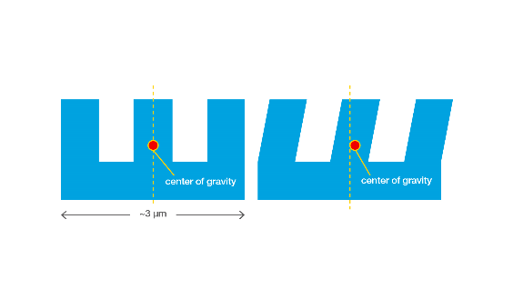
Alignment marks are specially designed gratings that are created on the wafer alongside each layer’s pattern. They are made up of lines with vertical sides that are perpendicular to the wafer’s surface. However, natural variations in the chip production process mean that sometimes the sides aren’t fully perpendicular but are instead tilted.
“The challenge I worked on is quite simple: What is the position – or center of gravity – of a tilted feature?” explains Simon Mathijssen. “You could say it’s halfway between the top corners or halfway between the bottom corners. For perpendicular features, this is the same, but not for tilted features, which brings ambiguity.
“This is a real problem, because the alignment sensor uses multiple colors of light to determine the wafer’s position and, with this ambiguity, each color will give a different answer. So, we are uncertain where the wafer actually is. That can lead to critical errors such as short circuits and connection failures that stop the chip from working.”
Delivering stellar results
Since joining the company in 2011, Simon has spent much of his career finding new solutions to this and similar problems. Many of these solutions have been implemented in the ORION alignment sensor. Since replacing the previous SMASH sensor starting in 2017, ORION has established itself as ASML's wafer alignment technology platform for both DUV and EUV lithography systems. Compared to its predecessor, ORION is more accurate and less sensitive to the kind of process variations that can lead to tilted alignment markers.

“We are also looking at a similar issue in overlay metrology: How accurately can we measure various layers of a microchip on top of each other when the markers are deformed? The big difference is the number of marks. For wafer positioning, there are tens of alignment markers. For overlay, there could be over 1,000,” Simon adds.
From fixing TVs to enabling nanotechnology
According to Simon, the foundation for his career was laid by his father, who would let Simon help repair TV sets as a child. “At that time, a television was quite a big, complex technological system. You could open it up and explore – that was fascinating,” he remembers.
After obtaining a PhD in organic electronics from Eindhoven University of Technology (TU/e), Simon joined ASML in the Sensors, Metrology and Control group – where he says he learned a lot about optics from his experienced and helpful colleagues. Currently, Simon is an important link between customers using ASML’s most advanced systems and the company’s metrology research.
“It was actually through interaction with customers that we realized mark deformation existed in the first place,” he says.
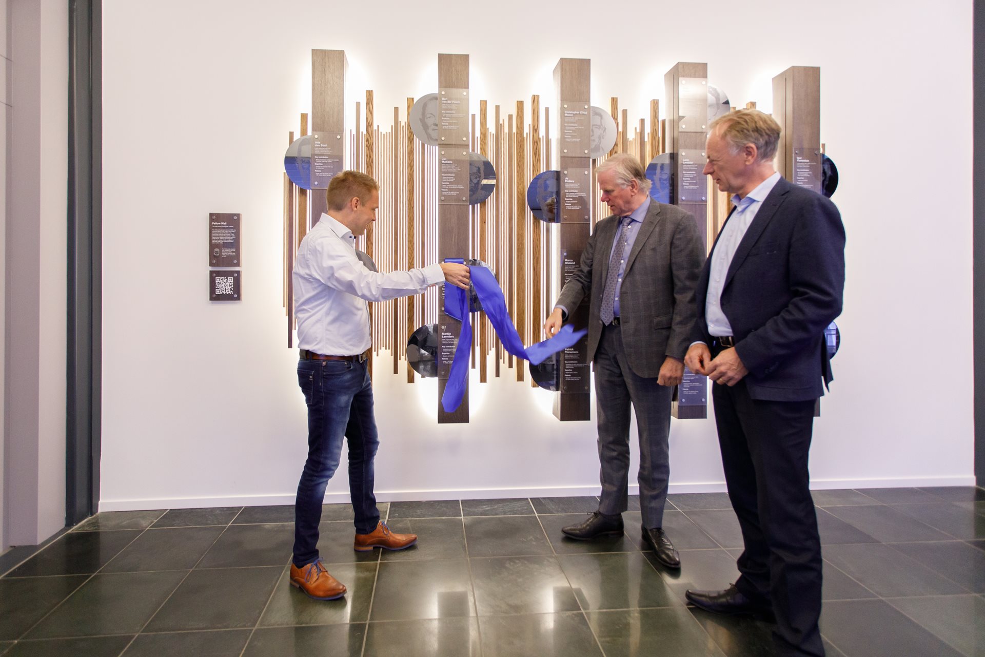
In recognition of the importance of his work, Simon was made an ASML Fellow at the 2021 ASML Technology Conference – an exclusive reward for the best and brightest technical talents whose groundbreaking ideas, key intellectual property and proven track record of publications have contributed to the company’s success.

Want to meet all our Fellows and learn about the ASML Fellowship program?


