Physics is at the heart of everything we do at ASML.

How does extreme UV lithography work?
Explore the physics inside the world's most advanced lithography system

Light source
Optical column
Reticle
Vacuum chamber
Wafer handler
Wafer stage


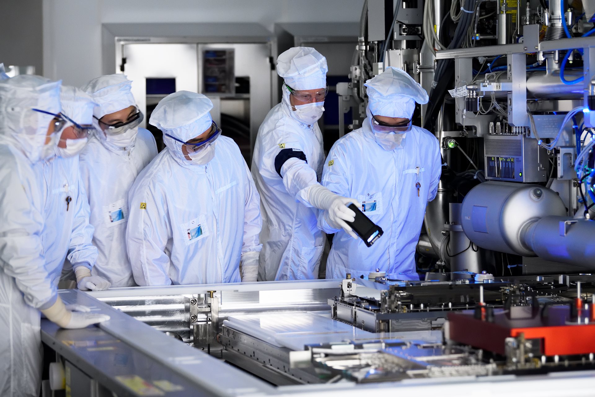
As a physics engineer, you could research how temperature fluctuations affect the projection of light or analyze the behavior of tin droplets when they are exposed to CO2 laser light.
You could also solve contamination issues by applying surface and interface physics. Or you could be drawing on all your physics knowledge to help improve the imaging, overlay and productivity of our tools. The possibilities of our physics jobs in R&D, Manufacturing and Customer Support are endless.
Physics meets mechatronics
Using models and algorithms to control for the physical effects that occur when measuring and exposing a wafer inside our lithography machines
In an ASML lithography machine, the wafer stage simultaneously moves two wafer tables, each holding a silicon wafer. While one wafer is being exposed, the position of the other wafer is measured by the machine’s metrology sensors, which saves time and increases yield. This dual-stage system architecture is called TWINSCAN.
The synchronized movement of the wafer stage, reticle stage (containing the blueprint of the pattern to be printed on the chip) and optics elements produces a number of physical effects that must be compensated for in order to maintain the machine’s nanometer precision and high productivity.
To do this, our physicists develop physical models and empirical algorithms that describe what’s going on inside our lithography machines and perform corrections for unwanted physical effects.

Read more
Indistinguishable from magic
In this story, three physicists describe what it was like to develop breakthrough technology – the EUV pellicle – that combats pattern defectivity in chipmaking.

"To be able to produce patterns on a nanometer scale, I work daily with engineers from all different kinds of technical fields and with lots of different physics principles. Getting to know our machines and combining all these different fields of expertise is by far the most challenging part of my job."
-Lisanne Coenen, system engineer, MSc in applied physics