5-minute read - by Kate Brunton, September 14, 2022
UPDATE: At a SPIE conference in September 2022, Vadim, Carmen, Guido and six other ASML employees were presented with a BACUS Prize Award “in recognition of their work in the research, development and commercialization of EUV pellicles for high-volume manufacturing.” See the LinkedIn post.
The pellicle is one of the breakthroughs that enabled EUV (extreme ultraviolet) lithography in high-volume microchip manufacturing. In this story, three physicists describe how ASML researched this ‘impossible’ technology and brought it to market.
“Any sufficiently advanced technology is indistinguishable from magic.” – Arthur C. Clarke, British science fiction writer
ASML’s most advanced pellicle seems impossible when you hear about it. A super-thin membrane, 13 nanometers thick (for reference, a human hair is approximately 80,000–100,000 nanometers thick), that lets through extreme ultraviolet (EUV) light whereas most substances absorb it, and that can withstand temperatures of up to 500 degrees Celsius in a high-vacuum environment? It seems unfathomable that this delicate, shimmering film could be so robust, but it is.
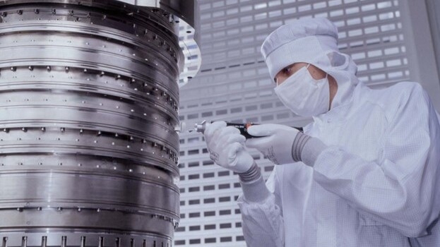
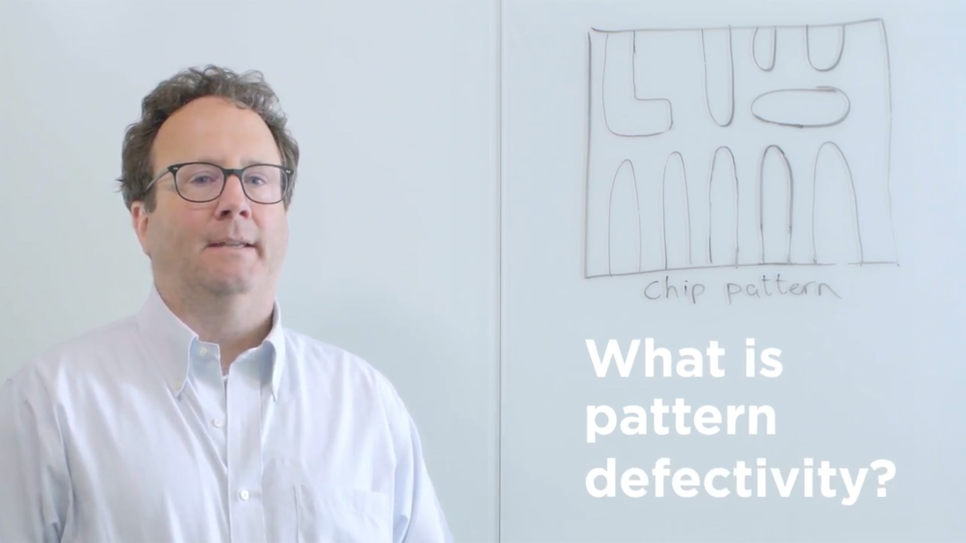
Pellicles are used in chipmaking as a way of reducing pattern defectivity. They are positioned inside the lithography machine just below the reticle, or mask (which is much like a stencil containing the blueprint of the pattern to be printed on the wafer), and their job is to catch miniscule particles that would otherwise cling to the reticle and end up printed on the wafer, causing the chip to fail.
ASML has been using pellicles for a long time in DUV (deep ultraviolet) lithography systems, but the stakes were raised when we developed EUV lithography technology. To transmit light of just 13.5 nanometers, the EUV pellicle had to be thinner and be able to withstand much higher temperatures inside the machine.
No one knew if it was possible, but we were keen to try.
'Aha' moments
“We had been working on thin films in the Research department since 2004, because we wanted to have a very thin membrane for a spectral purity filter that would only allow the right light wavelengths into the system,” says Vadim Banine, who at the time was a research project manager (he’s now head of Development & Engineering at ASML Berlin). “And now we wanted to see if we could apply the same technology to make an EUV pellicle.”
According to Vadim, his ‘aha’ moment came while he was watching a documentary on Japanese katana swords. “They make the swords with a lot of layers of steel,” he describes. “[The] next day I talked about it with a colleague of mine who was producing this thin membrane and he said, ‘Well, that’s a good idea. Let’s try this.’ He made a phone call and in two weeks we had a first sample.”
Vadim and other ASML researchers worked for many years with partner knowledge institutes to modify and improve the concept, running ‘imaging impact evaluations’ to test its validity. Armed with their research, they managed to convince ASML’s CTO Martin van den Brink that it was worth getting the Development & Engineering (D&E) department involved in designing and testing a full-scale EUV pellicle for use in high-volume manufacturing.
Passing the baton
“As soon as D&E joined the party, it scaled very fast,” Vadim recalls. But ASML still needed customer commitment for the pellicle to become a reality.
Carmen Zoldesi, who at the time was a reticle defectivity project manager (she’s now the design engineering and architecture line manager for light source performance in San Diego, California), explains that ASML found this support in Intel and other EUV customers. “In 2013, we were presenting our results in quarterly meetings with customers and at some point, it became obvious that it had some potential,” Carmen recalls.
Pellicles are particularly interesting for Logic chipmakers because the CPUs and other processors they manufacture are larger than Memory chips and more complex, sometimes involving hundreds of process steps to produce. If one Logic chip fails due to a defect, the economic impact for our customers is relatively high.
“After that, my department manager came and asked me if I wanted to stay with my old project or do this new project on the EUV pellicle,” says Carmen. “Even though it was still pretty small and we weren’t sure if it was going to work, I went with the pellicle. I like challenges.”
According to Carmen, it took years of persistent effort to see positive results and to finally win Martin van den Brink over to the idea of an EUV pellicle. “Martin was not a believer in pellicles,” she remembers, smilingly. “He was like, ‘This is never going to work.’ But we kept showing our progress, and at some point, he changed his mind. By 2014, I was presenting at SPIE.”
In 2016, the team released the first generation of EUV pellicles based on the multi-layered concept. They contained a core polycrystalline silicon (p-Si) layer bringing mechanical strength and several functional layers enhancing the pellicle’s performance, including cap layers keeping the film stable and barrier layers ensuring that all layers worked together.
New challenges
However innovative, this stacked concept was flawed. Building up multiple layers meant the pellicle was bound to thicker membranes, and stacking layer on layer to build up the film made for a complex production process.
Guido Salmaso joined the team in 2016 and later became the product system engineer for EUV pellicles. He describes finding out that the initial concept wasn’t as robust as they’d thought: “It was really a setback,” he recalls. “Customers were expecting the new generation of high-transmissivity pellicles at the beginning of 2019, but they weren’t going to get it.”
Guido had the unpleasant task of relaying this information to Martin van den Brink and Christophe Fouquet (then executive vice president EUV) in a meeting. “Of course there's the moment when you're asked, ‘Why didn't you see this coming?’ Why weren’t you able to predict that this concept would fail?’ But they also understood that in fields like the EUV pellicle, ‘failing’ is not a surprise, because it’s groundbreaking research and development.”
So, it was back to the drawing board – or in this case, the periodic table. “The problem is that there aren’t any materials that are completely transparent to 13.5 nm radiation,” says Guido. “Whatever you put in the path of the light will cost you photons, meaning customers will lose productivity.”

“Eventually, we managed to find a concept that worked,” he says. The team decided to combine all the functions of each layer into one composite membrane, believing this would solve some of the limitations of the previous concept because it would be possible to deposit more transparent membranes, which would lead to higher transmission. The result was a silicide composite pellicle that proved to be both transmissive and robust.
“It was a breakthrough that relied on the work that had already been done in Research, and it really took us a big step ahead of the previous generation,” says Guido.
An enabler of EUV
The pellicle is one of the breakthroughs that brought EUV lithography to high-volume manufacturing. It was also one of the many innovations that led Vadim Banine and Erik Loopstra to be recognized with a European Inventor Award by the European Patent Office in 2018.
“EUV has a lot of things which look like magic,” says Vadim. “The pellicle was just one of the many 'impossible' things that turned out to be possible.
“The current EUV pellicle has evolved a lot and looks quite different from the original one. The idea and first proof was just the beginning of the work. After this it took eight years, many more people and fanatical dedication to realize it.”

A physicist’s playground
There are plenty of challenges like the EUV pellicle for physicists to work on at ASML. “I think it’s a good background to have at ASML,” says Carmen. “You have the opportunity to dive deep into one topic, or to have more of a system-level overview.” Carmen is currently hiring plasma physicists for her team that focuses on the performance of the EUV source in San Diego, California.
Guido adds: “You really have the opportunity to do fun stuff in physics. It's also formative, because you will fail for sure, but you learn how to fail and how to learn from those failures.”
See our vacancies for physicists or learn more about pushing the boundaries of technology in physics and R&D at ASML.