
4-minute read - by Kate Brunton, October 11, 2023
Wilton has been an important source of innovation in the semiconductor industry since the 1960s. Starting with Perkin-Elmer’s Micralign, continuing with Silicon Valley Group’s Micrascan, and later with ASML’s TWINSCAN scanners, including extreme ultraviolet (EUV) technology, lithography owes much of its innovation to Wilton.
1. ASML Wilton has its roots in the beginnings of the chip industry.
Before it became ‘ASML Wilton’ in 2001, this Connecticut site was part of Silicon Valley Group (SVG), and before that, it was part of Perkin-Elmer.
Our story begins in 1937, when two men who shared a passion for astronomy and physics founded Perkin-Elmer. They were Richard Scott Perkin, an entrepreneur, and Charles Elmer, a court reporter. Perkin-Elmer specialized in precision optics for a wide range of applications, from World War II reconnaissance systems to medical imaging components. They were even responsible for the CO2 sensor that saved the astronauts during the Apollo 13 failure.
2. The first optical lithography machine was invented in Wilton.
The first integrated circuits consisted of features of 200 microns (about the width of two human hairs) printed using contact lithography. In that technique, a reticle, or mask, containing the pattern to be printed is pressed onto the surface of a silicon wafer, much like a stamp. Contact lithography achieved good printing resolution, but the process inherently created defects. Small bits of dirt or coating from the wafer would stick to the reticle, ruining the pattern for subsequent chips. Many of the chips from each wafer would malfunction.
In response to this, Perkin-Elmer developed a lithography technique called projection lithography. This device was essentially a large photocopier system. Harold Hemstreet, a Perkin-Elmer employee, was convinced that he could simplify the optics in the system and secured support from the board of management to pursue the idea. Using that support, in 1972 Abe Offner developed the ‘Offner relay’, an optical system that used mirrors instead of lenses.
Using this new system, Perkin-Elmer created the ‘projection scanning aligner’, or Micralign, which drastically increased the number of working chips on a wafer. They shipped the first Micralign to Texas Instruments in 1973 for $95,000 (around $650,000 in today’s money) and within six months, the machines were paying for themselves. Perkin-Elmer quickly became the most important lithography supplier in the world.

3. The Micralign traces its origins to the US military.
During World War II, Perkin-Elmer built panoramic reconnaissance cameras for the CIA and the US Department of Defense. The company continued their involvement with the US military through the 1950s and 1960s. During that time the US Air Force increasingly relied on microchips, but by the late 1960s, the semiconductor industry was struggling to develop more advanced methods of producing them. The Air Force asked Perkin-Elmer to create a ‘projection mask aligner’, and that work kickstarted the R&D that led to the Micralign.
4. Wilton has enabled Moore’s Law again and again.
In 1965, when Gordon Moore predicted that the number of transistors on a microchip would double every two years, the available lithography equipment couldn’t support such a bold estimate. Yet over time, his prediction became a kind of self-fulfilling prophecy that still propels the semiconductor industry forward to this day.
Wilton’s first contribution to Moore’s Law was the Micralign, which enabled immense progress in microchip manufacturing in the 1970s and 1980s. Perkin-Elmer sold its lithography division to SVG in 1990, and later that year, SVG introduced its next revolutionary lithography system: the Micrascan, which was the industry’s first step-and-scan lithography tool, or simply ‘scanner’. Scanners provided the next big leap in microchip production and are still the industry standard today.

5. ASML is carrying on Connecticut’s rich manufacturing legacy.
Once called the ‘provision state’ by the first president of the United States, Connecticut was a leader in manufacturing throughout the 19th and early 20th centuries. It produced products ranging from auto parts to clocks, buttons, textiles and silverware. Today, ASML Wilton’s high-precision factory cleanrooms carry on the state’s manufacturing legacy.
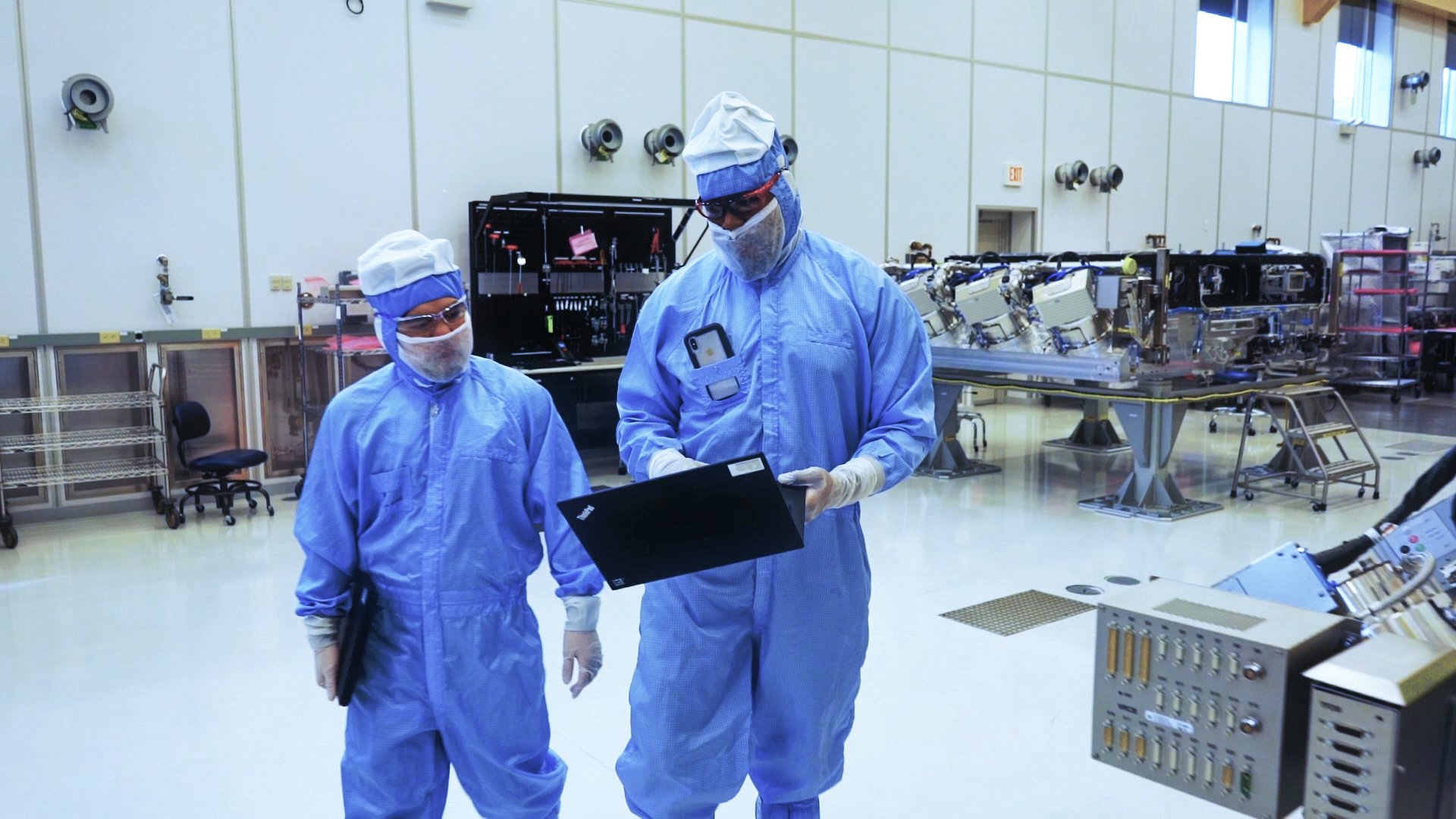
Around 1,300 colleagues work in manufacturing in Wilton, in roles ranging from entry-level optical technicians to experienced engineering positions. 'Concurrent engineering' stations located on the factory floor enable engineers and technicians to work side by side on new developments within fully functional test modules.
ASML Wilton was recently featured on local News12’s Made in Connecticut program, and was inducted into the Connecticut Manufacturing Hall of Fame.
6. Today, the top modules of ASML’s next-gen EUV machines are built in Wilton.
The ‘top module’ of our TWINSCAN EUV lithography machines contains the reticle stage and reticle handler. This contributes to overall machine performance by facilitating the precision, accuracy and increased throughput chipmakers require to make the next generation of computer chips.
Top modules are shipped from Wilton to our headquarters in our headquarters in Veldhoven, the Netherlands, where they are integrated into the complete lithography machine.
7. There are still 300 Micraligns in use today.
Technology developments in the semiconductor industry rarely become obsolete. Although progress drives ever forward, chipmakers still use mature technology to fabricate many of the chips found in the latest devices.
Of the 3,000 Micraligns ever shipped, around 300 are still in use at chipmaker fabs around the world. ASML Fellow Chip Mason recently gave a talk at SPIE celebrating the 50th anniversary of Micralign, and he and many other original ‘Wilton Micraligners’ from the Perkin-Elmer days still work at ASML. When Chip was asked to give his commemorative talk, his team was able to locate a Micralign in someone’s attic and ship it to California for the occasion.


