EUV lithography does big things on a tiny scale. The technology, which is unique to ASML, prints microchips using light with a wavelength of just 13.5 nm – almost x-ray range. EUV is driving Moore’s Law forward and supporting novel transistor designs and chip architectures.
Leading-edge microchips contain billions of transistors. With each new generation (often referred to as a ‘node’), chipmakers pack in ever more and tinier transistors to make the chips more powerful, faster and energy efficient. Chips made with EUV lithography are enabling smart technology (cars, phones and homes), augmented reality, artificial intelligence and much more.
EUV lithography is important because it makes scaling more affordable for chipmakers and allows the semiconductor industry to continue its pursuit of Moore’s Law. EUV systems are used to print the most intricate layers on a chip, with the rest of the layers printed using various DUV systems. Both types of technology will be required in parallel for many years to come and we’re continuing to advance both technologies.

Mass producing leading-edge microchips
If you have a relatively new smartphone, one of the latest gaming consoles or a smart watch, it’s likely you’ve benefited directly from EUV lithography technology.
EXE systems
EXE systems are the latest generation in EUV lithography. The underlying technology is known as ‘High NA’, which stands for high numerical aperture. With an (NA) of 0.55, their innovative new optics use our novel 13.5 nm EUV light source to provide higher contrast and print with a resolution of just 8 nm.
The EXE platform will support high-volume chip manufacturing in 2025–2026, enabling geometric chip scaling into the next decade. That will include future advanced nodes, starting at the 2 nm Logic node and followed by Memory nodes at a similar density. By reducing the number of process steps in high-volume manufacturing, chipmakers will benefit from significant reductions in defects, cost and cycle time.
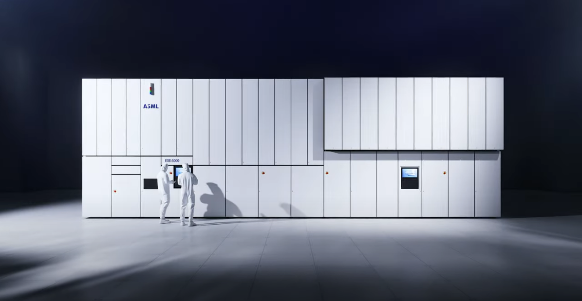
 TWINSCAN EXE:5000
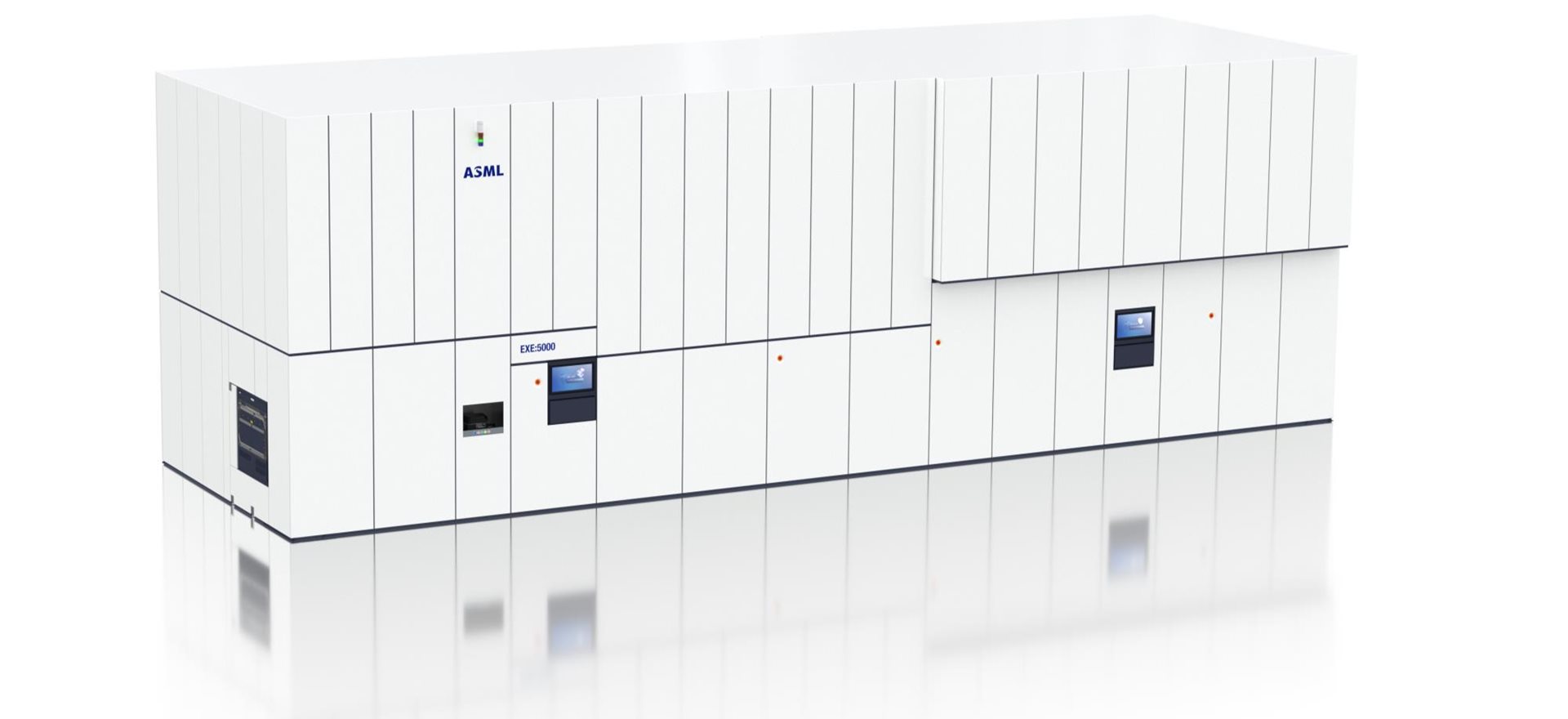
The dual-stage extreme ultraviolet (EUV) lithography system is the first in a new generation of machines that will support advanced Logic and Memory chip production.
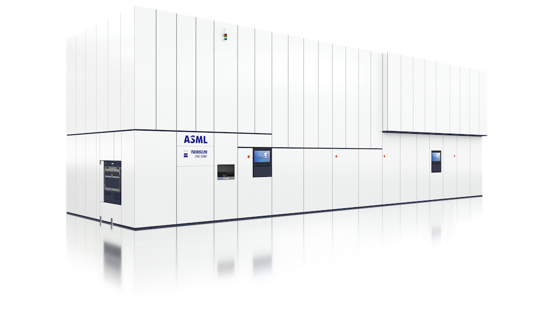 TWINSCAN EXE:5200B
The dual-stage EUV lithography system is designed to support volume production of sub-2 nm Logic nodes and leading-edge DRAM nodes.
NXE systems
NXE lithography systems are used in high-volume manufacturing of advanced Logic and Memory chips. They’re the first systems to use our novel 13.5 nm EUV light source, and they have a numerical aperture (NA) of 0.33. These systems print microchip features with a resolution of 13 nm, which is unreachable with deep ultraviolet (DUV) lithography. Chipmakers use our NXE systems to print the highly complex foundation layers of their 7 nm, 5 nm and 3 nm nodes. Read about how EUV lithography went from imagination to reality.
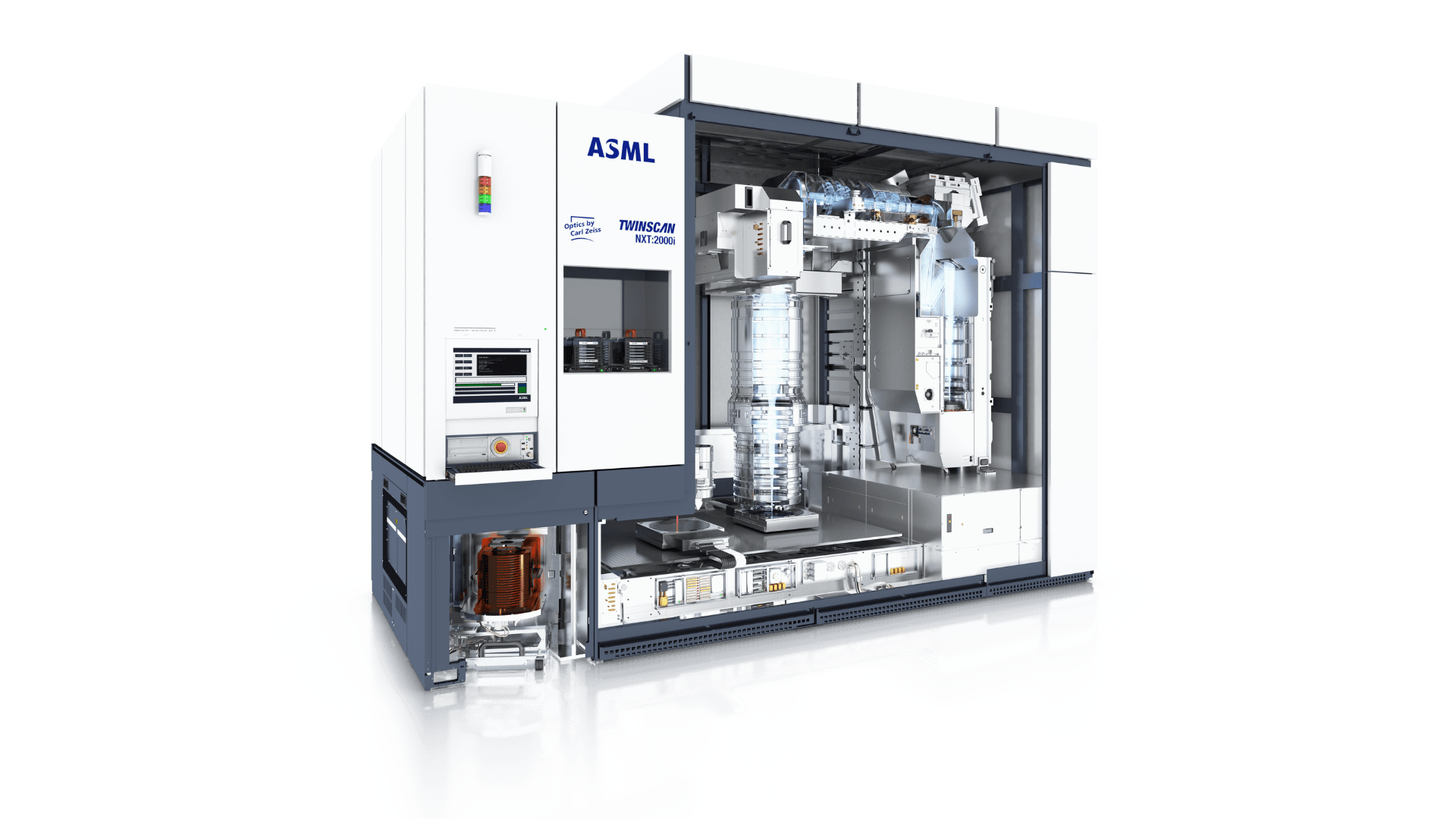
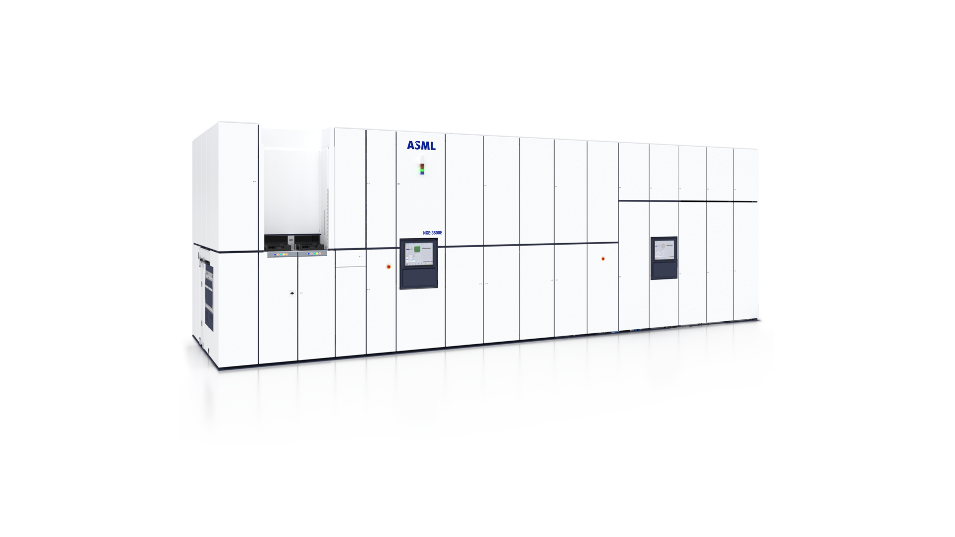 TWINSCAN NXE:3800E
The dual-stage EUV system supports high-volume manufacturing of 2 nm Logic nodes and leading-edge DRAM nodes.
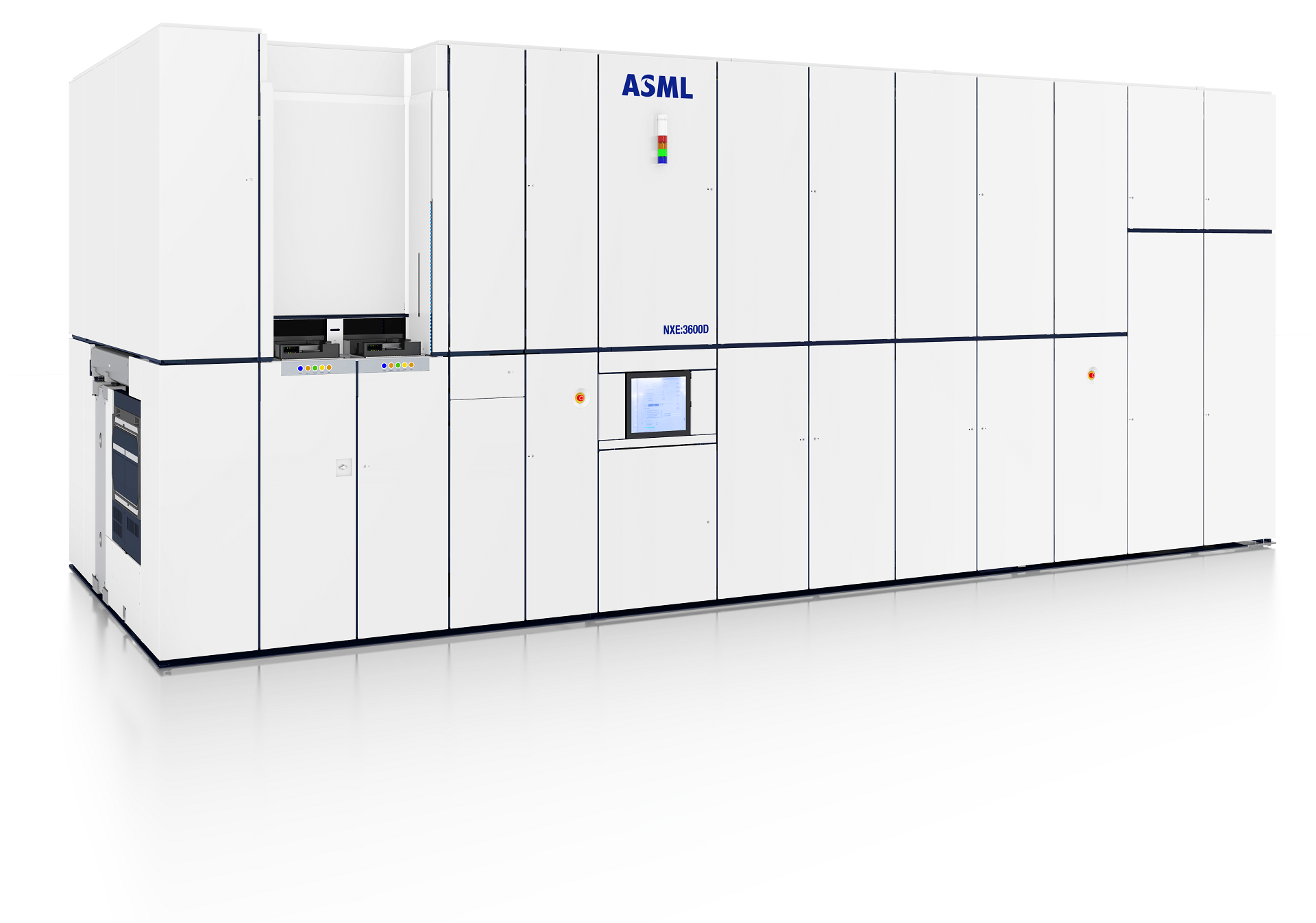 TWINSCAN NXE:3600D
The TWINSCAN NXE:3600D supports EUV volume production at the 5 and 3 nm Logic nodes and leading-edge DRAM nodes.
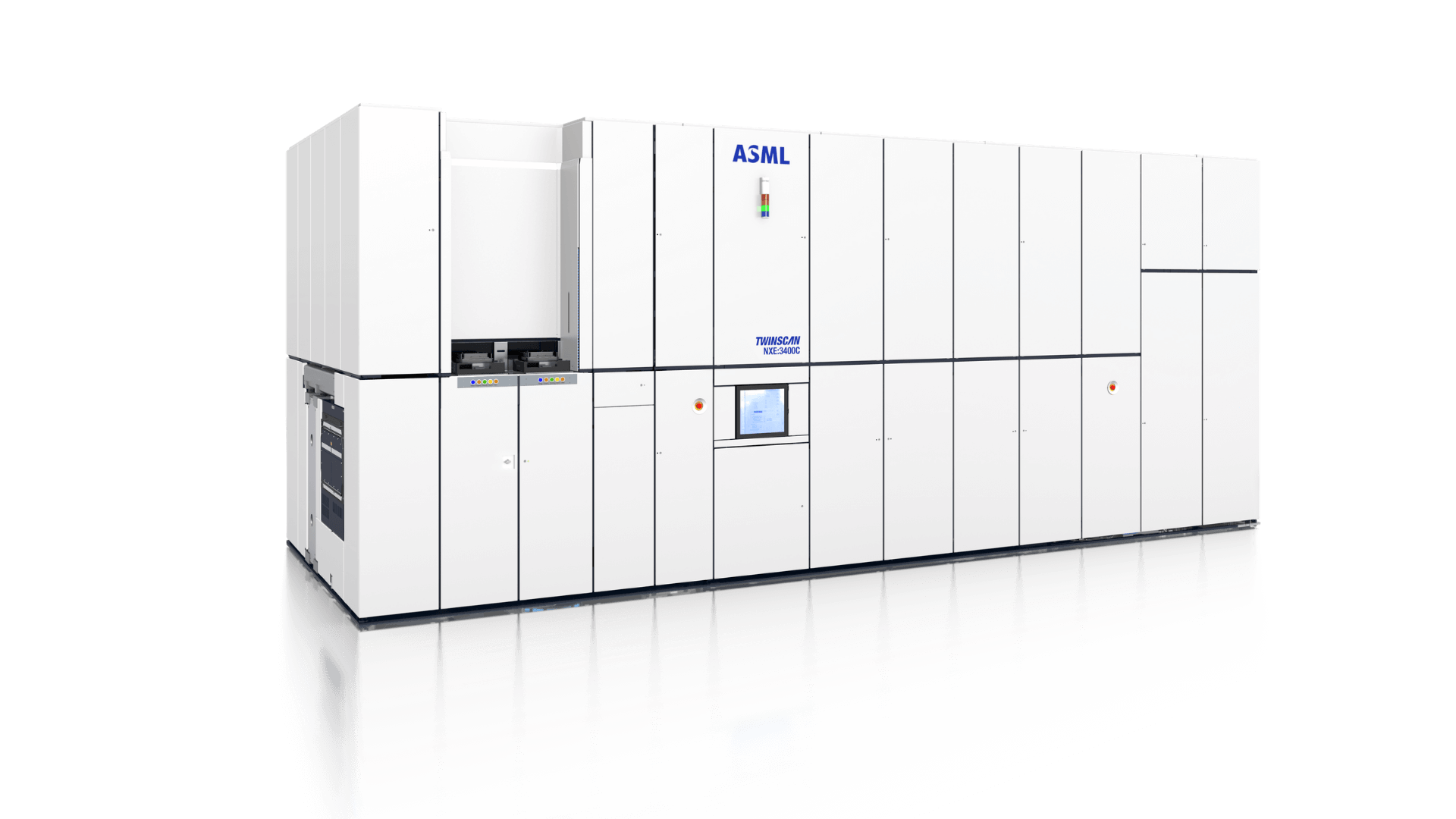 TWINSCAN NXE:3400C
The TWINSCAN NXE:3400C lithography system supports volume production at the 7 and 5 nm nodes.
How does EUV work?
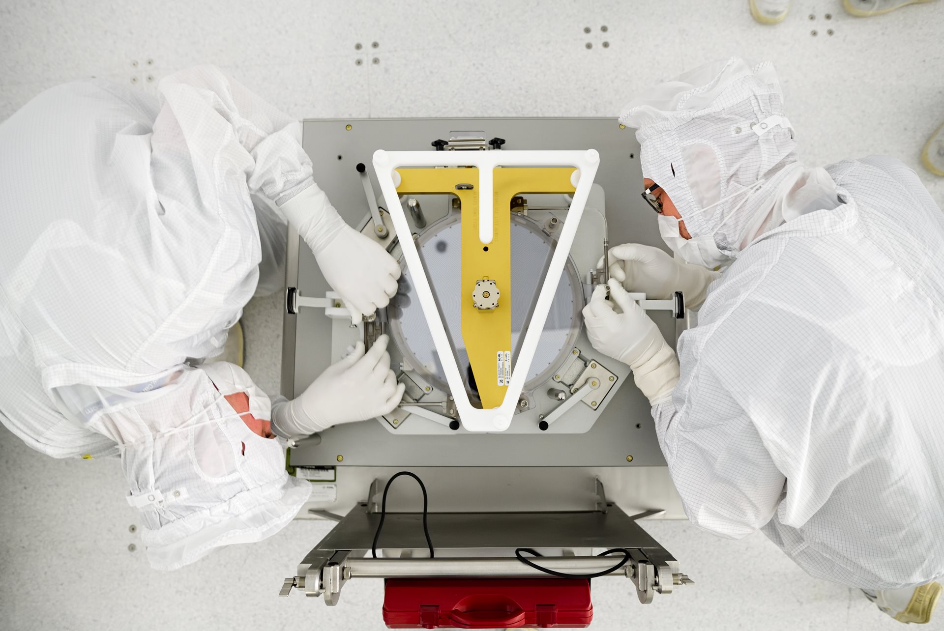
Explore inside an NXE lithography system

Light source
Optical column
Reticle
Vacuum chamber
Wafer handler
Wafer stage


The road to EUV
EUV technology took more than two decades to develop
Engineering EUV was anything but simple. ASML invested more than €6 billion in EUV R&D over 17 years. We acquired Cymer – a company specialized in light source technology – to accelerate EUV source development. And once the technology was developed, we had to overcome numerous technical challenges to meet chipmaker’s requirements for high-volume manufacturing.

How EUV lithography was developed